💬 MysXLedDimmer
-
roooh...that's cool :)
-
@tbowmo I really like this (and your other) designs, because for a beginner like me, they are easy to modify and to extend.
I'm currently designing a 3 channel Version with MYSX, but I'm not sure the IRLML2502 is suited for my task.
The maximum continous load needed is 2 A at 12 V (~24 Watts LED). The voltage at the gate (from the atmega) is 3.3 V.
According to the datasheet the maximum current for this part is 4 A (pulsed, with a given duty circle).
I feel that this tiny little MOSFET is not capable to drive 12V and 2 A continous, but I'm not yet smart enough to calculate it.
I'm currently using IRLIZ44N which work fine with ~5 V at the gate but for my new layout I will omit the 5V line and will use 3.3 V and therefore need to switch the MOSFET.
So my questions:
-
Have you thought (calculated) the current your design is capable to handle?
-
Does someone has a link for me where the calculation for my "feelings" are described in an easy way? I know the difference between I, U & R (most of the times) but I'm no expert and still try to learn. ;-)
-
-
I haven't done any calculations on the transistor, just looked at some existing designs, where it was used..
I haven't even come to the point where I build it yet.. (even though it has been on openhardware for quite some time now). currently I'm waiting for a first batch of prototype pcbs with the sensebender micro mk2, where this board also is incorporated on the same panel.
Also, components are on their way from china.. :)
btw. MysX only specifies 2 PWM channels, so where do you fit in the extra for a 3 channel dimmer board?
-
@tbowmo I really like this (and your other) designs, because for a beginner like me, they are easy to modify and to extend.
I'm currently designing a 3 channel Version with MYSX, but I'm not sure the IRLML2502 is suited for my task.
The maximum continous load needed is 2 A at 12 V (~24 Watts LED). The voltage at the gate (from the atmega) is 3.3 V.
According to the datasheet the maximum current for this part is 4 A (pulsed, with a given duty circle).
I feel that this tiny little MOSFET is not capable to drive 12V and 2 A continous, but I'm not yet smart enough to calculate it.
I'm currently using IRLIZ44N which work fine with ~5 V at the gate but for my new layout I will omit the 5V line and will use 3.3 V and therefore need to switch the MOSFET.
So my questions:
-
Have you thought (calculated) the current your design is capable to handle?
-
Does someone has a link for me where the calculation for my "feelings" are described in an easy way? I know the difference between I, U & R (most of the times) but I'm no expert and still try to learn. ;-)
@TimO I think you are safe ;-) To translate this to I, U, & R, look at these pictures taken from the datasheet
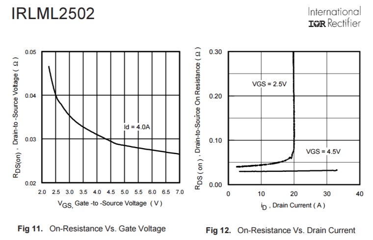
At 3V gate source -voltage Rds is less than 0.04 Ohm. With a current of 2A the dissipation in the FET will be I^2 * R = 2^2 * 0.04 = 160mW -
-
@TimO I think you are safe ;-) To translate this to I, U, & R, look at these pictures taken from the datasheet
At 3V gate source -voltage Rds is less than 0.04 Ohm. With a current of 2A the dissipation in the FET will be I^2 * R = 2^2 * 0.04 = 160mW@AWI Thank you! With a maximum rating of 1.25W for this tiny FET I'm indeed safe.
@tbowmo I'm using MYSX_D4_INT for the third FET. I've looked at @Anticimex MySensors node where it is connected to Arduino Pin 3.
-
@AWI Thank you! With a maximum rating of 1.25W for this tiny FET I'm indeed safe.
@tbowmo I'm using MYSX_D4_INT for the third FET. I've looked at @Anticimex MySensors node where it is connected to Arduino Pin 3.
-
@Anticimex correct, but you have a board with MYSX 1.5 which I've studied. Sadly there is no other MYSX Atmega328p based board (yet).
-
@Anticimex correct, but you have a board with MYSX 1.5 which I've studied. Sadly there is no other MYSX Atmega328p based board (yet).
-
@Anticimex I'm sorry for the confusion! I've not found any mapping from the MYSX pins to the arduino pins, so I've looked into your board mentioned above and there I found out, that D4_INT is connected to PD3/D3 on the Atmega328p/Arduino Pro Mini. D3 is also capable of PWM. I know, this won't mean that D4_INT on other boards will be capable of PWM.
@TimO I see. But the pin on MYSX you connected it to is not marked as pwm capable so if you have a daughter board that expect pwm on that pin it would not be "MYSX compatible" as in that it would not work on other MYSX motherboards.
-
It's purely up to the person who is creating a board, how to map pins for the MysX connector! What is done on the board by @Anticimex is probably not what I would do, if I made a board.
What MysX states, is the capabilities the different pins should have, not how they are mapped to an atmega328, atsamd21, esp8266 or stm32 micro processor!
-
@Anticimex I'm sorry for the confusion! I've not found any mapping from the MYSX pins to the arduino pins, so I've looked into your board mentioned above and there I found out, that D4_INT is connected to PD3/D3 on the Atmega328p/Arduino Pro Mini. D3 is also capable of PWM. I know, this won't mean that D4_INT on other boards will be capable of PWM.
@TimO my board maps the pin functions described by MYSX to corresponding pins on the atmega. That does not mean you have to map it just like that, but the principle of MYSX is that a daughter board can be designed based on the MYSX pin functions and therefore expect a motherboard to be able to provide the logic functions described by each pin.
-
I do understand that! :D For a Atmega328 the possibility is high that D4_INT is mapped to D3.
The atsamd21 is capable of PWM on every pin?! (I've no experience with atsam).I will only need two dimmer and one switch port. So, if I wanted my board to be "MYSX compatible" which digital output pin on the MYSX do you suggest to use? As it is a mother-/daughter board design I'm working on the complete 2.6 MYSX is available.
I'm tinkering on a LED dimmer daughter board that will be able to get stacked on top of a atmega328p motherboard. The atmega328p motherboard is based on the layout (size, position of MYSX ..) of the sensebender gateway. The idea is, that the daughterboard may be used on top of the sensebender gateway if a mcu with more horse power is needed, for example for a combination of gateway & sensors. The atmega328p based board is suited for simpler tasks.
-
Well, my board is fully compatible, but mind that it uses MYSX 1.x so you need to have a close look at the pinout of MYSX 2.x.
I am not sure what you mean with "which digital output pin on the MYSX". All pins marked 'D' are digital in nature. You can use anyone you want on your daughterboard.
Your mainboard is expected to connect for example, D4_INT to a pin that is capable of interrupts and digital IO. Which one, is up to you as motherboard designer. -
Well, my board is fully compatible, but mind that it uses MYSX 1.x so you need to have a close look at the pinout of MYSX 2.x.
I am not sure what you mean with "which digital output pin on the MYSX". All pins marked 'D' are digital in nature. You can use anyone you want on your daughterboard.
Your mainboard is expected to connect for example, D4_INT to a pin that is capable of interrupts and digital IO. Which one, is up to you as motherboard designer.@Anticimex okay! So I will stick to D4_INT for the third channel and it will be MYSX compatible as long as my daughter board uses it as digital io. In some combinations, like your MySensors node, the sensebender gateway and the board I'm working on it is also capable of PWM on this pin, but that is not how it is specified by the specification. That's okay for me!
I really like the idea of the MYSX and hope more boards will support it in the future! -
@Anticimex okay! So I will stick to D4_INT for the third channel and it will be MYSX compatible as long as my daughter board uses it as digital io. In some combinations, like your MySensors node, the sensebender gateway and the board I'm working on it is also capable of PWM on this pin, but that is not how it is specified by the specification. That's okay for me!
I really like the idea of the MYSX and hope more boards will support it in the future!@TimO Yep, that sounds right. It will probably be quite common that the micro will have more capabilities on the various MYSX pins than the MYSX spec states the pin in question can handle, but I tried to spec MYSX to be as compatible as possible with a range of micros so it is quite "stupid" in it's pin featureset.
It is basically the same reasoning for the connector. It is large and bulky and hard to use in really small boards, but I wanted it to be easy to use, and easy to source. And it provide a nice debug interface when left unconnected. Tradeoffs, tradeoffs. :)
Hello! It looks like you're interested in this conversation, but you don't have an account yet.
Getting fed up of having to scroll through the same posts each visit? When you register for an account, you'll always come back to exactly where you were before, and choose to be notified of new replies (either via email, or push notification). You'll also be able to save bookmarks and upvote posts to show your appreciation to other community members.
With your input, this post could be even better 💗
Register Login