💬 No neutral power supply/relay board for in wall switch
-
-
@openhardware-io
Great design! I first looked at the Power Integration devices some time ago when I was trying to understand why my wireless thermostat receiver had stopped working (o/p cap gone high ESR). The original design from Power Integrations was for a Bluetooth enabled switch, but this is a nice simplification. It's worth looking at the original design notes to understand how this uses 'leakage current' through the load to drive the switch mode power supply. As far as I can see. the TI TPL7407 device driving the relays was not originally designed as a touch switch, but with its CMOS compatible inputs I presume it works OK with the leakage current from the live mains.
Tony -
interesting just bought some sonoff no neutral light switches needs a cap across the live / neutral is rgis the same ?
This board uses the same working principle behind the scenes as the Livolo or Sonoff no neutral switches (some use a triac based implementation). But again the idea is the same - we take advantage of the leakage current from the light bulb. So yes it still requires a capacitor across the bulb in some cases. This is because we power everything via the light bulb which is in series with our circuit and in the end it all comes down to physics law.
So no @arden , this one is not so different compared to the one that you already have. I did this because I'm a more of a diy person and I like to customize stuff and of course learn from it.
Another advantage is that you don't depend on external or 3rd party stuff and you can build/customize it whenever you want (of course this means that you know what you're doing considering the fact that you are dealing with the mains here).
As I live in EU I have only the live wire inside walls for light switches so this is another reason why. I know that there are another ways of accomplishing the same result but I don't want battery powered switches nor putting stuff on or inside my ceiling. -
Received my boards and started to perform some testing. It worked OK when powering front plates loaded with Bluetooth LE software which are drawing only ~500uA. But as soon as I tried to power a Bluetooth mesh node which draws constantly around 5-6mA then the stand-by supply (the one built around LNK364 IC) didn't acted fast enough when performing the switching causing the BLE mesh node to reset. In other words the power supply startup time was pretty slow for this kind of circuit.
After some serious investigations and headaches (around 3-4 days or so) I finally found why. It has to do with the AC-DC converter "capacitive loading". Initially I though that it was because of the output filtering capacitors and which are also used to store energy between cycling the bi stable relay on and off. As you all know capacitors are good for filtering the ripple and storing electric energy...BUT and very important for this project over here - if they're too big they make the power supply to react a little bit slow.
Why? The reason is very simple: if you use too large capacitors then it takes longer to charge (not to mention about high inrush currents) and because of that they slow down things affecting the AC-DC converter feedback loop.
Well, in a normal use of the power supply and when not cycling between on and off power states too fast this won't be noticed and doesn't matter too much. In my case it matters and guess what? - not the output capacitors were the culprit after tinkering a little bit with their values.
The input filtering capacitor was causing issues. Yes, I'm talking about the input filtering stage after the bridge rectifier. But in this case I started to "attack" the AC/DC power supply in a different way and that is: what happens at the input stage when the supply is switched on and off ?
Let's not forget that in this project the stand-by AC/DC converter is in series with the load (light bulb) and it "breathes" and draws power from the mains voltage and the leakage current from the light bulb which can be very small especially when using LED bulbs.
So what happens actually? As you all know the AC/DC converter won't work if the input AC voltage is less than 85V or so as most are rated to work between 85-265Vac right? But what this means after the rectifier/filtering stage where we have a continuous voltage (let's forget about ripple right now)?
Taking the minimum ac voltage value of 85V this translates to: 85 x 1.41 =~120Vdc. So untill the input filtering capacitor won't reach that dc voltage value the LNK364 chip won't work and here I'm referring to it's internal voltage regulator that powers the internal circuitry or it's "start up" circuit. (in reality it may be less than 120Vdc, but still...)But then you may think: yes, yes but the input filtering capacitor is only 4.7uF - won't it charge fast enough? Well no, and not quite - let's not forget that it's an electrolytic capacitor with higher ESR and not only that - what matters here the most is the fact that the leakage current from the light bulb dictates it's charging rate an that current can be very small !!!
And now you have it - the input capacitor in this case slows down things and affects the power supply start up time. And it doesn't matter that much if you increase the output capacitors and it becomes even worse because then we end up affecting the feedback loop from the converter.
So what I did was to remove completely the input filtering capacitor and now it's damn fast - yes the power supply still works as expected but it's much faster between on and off cycles. And if you look at the original Livolo switch it doesn't have it either but now I understand why.
We have enough filtering at the output stage so it won't affect our powered circuits. It's a little bit noisy at the input but not that much I would say because we have a bridge rectifier. And the load doesn't draw too much current so it should keep up without the input capacitor which also stores energy for the primary inductor. The LNK364 internal MOSFET shouldn't be affected as it's rated to support the peak input values and even more (700Vdc) as the input capacitor was averaging a little bit the rectified voltage waveform (but not that much anyways because it's small value). I will try with a 1uF/2.2uF and see if that slow things again.
So yes..I was almost ready to give up on this project. Now I'm more happy than ever and also because I learned new stuff. And designing/playing with offline AC/DC converters is kinda new for me. There are still many things to learn of course.
I also need to thank @axillent for its "AC-DC at own" post from where I got inspired a little bit.
-
As a side note: this doesn't mean that the input filtering capacitor is useless in the ac/dc power supplies as it also helps to store energy for the input stage which then gets transferred to the load by the pwm controller. Another useful thing is that it doesn't let the rectified wave voltage to drop too much which may not be very good for the input stage of the pwm controller making it to perform worse.
But in my case and particularly in this application it interferes when the switch "switches" between the two power supplies (well the other one is more of a "series regulator").
I will do some more tests. The most important thing for me right now is the power supply stability and then the thing I was waiting for the most: to create a 2 way setup using 2 switches to drive the same led bulb (for stairways).
-
As a general rule it seems that the input capacitor is choosed based on the needed output power which is obvious and the magic formula is (when using a bridge rectifier):
C (uF) = 2 x Pout (W)
So in my case one relay draws about 300mW when switching and we have two so let's take the worst case 600mW. Then the radio part and mcu should not take more than 30mW of power.
Summing up we have 630mW peak which translates to a 1.26uF capacitor and the nearest is 1uF.I just tested with 1uF and it works just fine without a glitch.
So yeah learning new stuff as I go along. I wanted for a long time to learn how to design offline AC/DC converters because the power supply is the most important part of every circuit and so often overlooked.
-
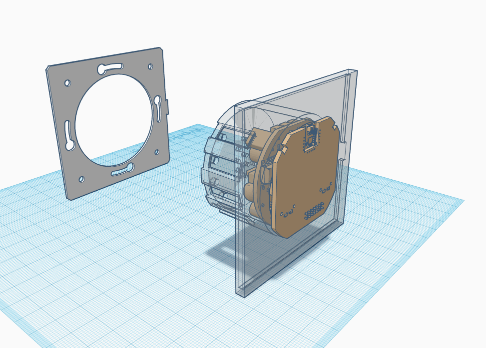
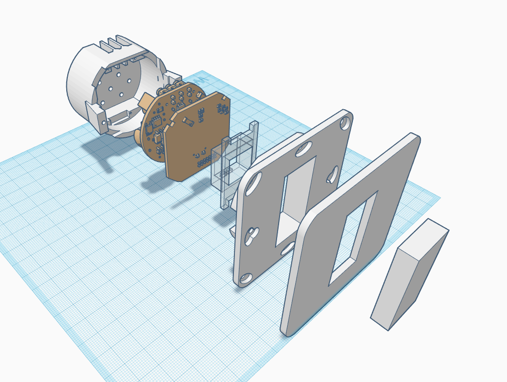
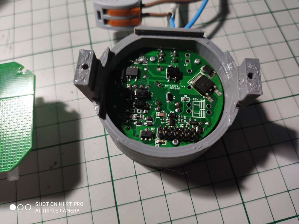
Started designing the enclosure for 3d printing ... I will use PET-G as it's pretty strong and not very flammable or so it seems after some tests. I don't know about electrical insulation properties yet ...This all very depends on what other compounds are used when it's manufactured.
-
I did some final testing and everything seems to work just fine so I can say that this is the final revision. The touch sensing board including radio/mcu must not draw more than 10mA (it will work but won't be stable).
I updated the BOM and schematic with required voltages for caps where it's more important - the rest are 10V or so not that critical (the ceramic caps should be X5R or X7R).
Oh and I replaced the 22uF/25V capacitor with a tantalum type. Initially I used a ceramic one and the board started to sing :smiley: . Well not quite..it was a more of a buzz because as you all know SMD multi layer caps are known to have this property.
Next step as already mentioned above is to design the enclosure which will be 3D printed with PETG. The front side will be a custom glass plate also which I'm thinking now how to make it look and fit better.
It works slow on my side because...well my free time available for this hobby is kind of limited.
-
Amazing project! I want to repeat it, but there is a problem. I can't find the T1 transformer where you bought it.
50pcs/lot EE10-A1 Switching Power Supply High Frequency Transformer 220V to 5-12V Maximum Output 3W
https://a.aliexpress.com/_sOShjHIt's the same supplier that I used also and the lot seems to be fine...well at least the 2 pieces that I tested so far :smile: .
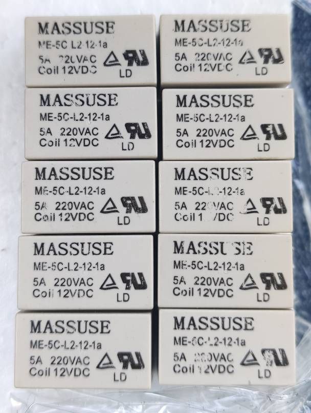
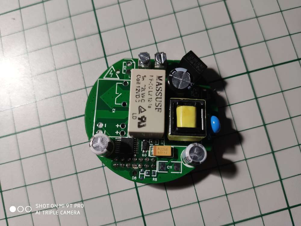
Now the latching relays. I found them on Aliexpress only and I received something else instead (which seems to happen from time to time) but luckily it works OK so far. So instead of Hongfa relays I got Massuse which seem to be equivalent.
Rest of the components can be sourced from LCSC which is a more trusty component supplier compared to various vendors from Aliexpress (which I already knew..but I didn't had other choices).
Oh and the PCB design and everything else was done using EasyEDA for obvious reasons (JLCPCB is very cheap and pretty good quality for a hobbyist, also their SMT service). I really like their ecosystem - you just create the design using their tool and order everything from there - very, very handy and cheap also as I already mentioned.
-
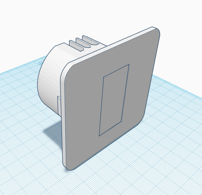
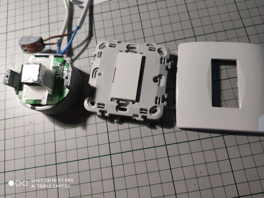
As promised the final design! This is for one channel which I will use mostly in my house. The backside is 3d printed and it holds the electronics. The front panel and fake button are bought from the local store (Leroy Merlin) and I like it very much (it's part of modular switches design and it's very cheap). I could 3d print the front side plastics..but it I can't get the same look and feel - can't beat the molded plastic with a 3d printer for now ... (well you could use some resin or other stuff to fill the holes and then spray paint but still it's a lot of work and it doesn't worth imho)
Here are some pictures from the design. I will post later the pictures with the real product also.
-
And the real product pictures now:
Short demo of touch functionality (will post later on the bluetooth mesh network functionality):
https://streamable.com/b52qb
https://streamable.com/dj3z7Sorry for the solder bridge replacing the R20 inrush current limiting resistor..that's just temporary until I get the real component :smile: . And yes, the capacitor across the bulb is still needed but it's a very small one of 0.1uF/250Vac and it should fit near the light bulb on the ceiling (only one is needed if there are two light bulbs on the same circuit).
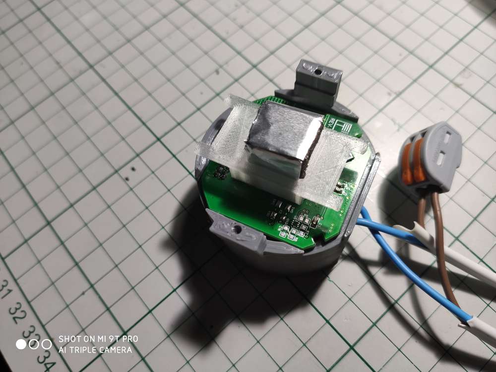
The aluminum foil wrapped around that sponge is to "extend" the capacitive sensor so that it reaches the front plate fake plastic button. The 3d printed clear plastic around it is to hold it in place and also to spread the small leds light.
Everything is custom made except for the front plastics.
-
@mtiutiu
congrats :clap:
I'm curious, are you happy with range (I noticed you changed a bit the rf reference design routing).
I guess you use BLE mesh regarding average power consumption (which should improve range too), so rfm69+mysensors is maybe too power hungry?
Well, I think I'll try to assemble a few of your boards, this might be the first design I try here :nerd_face:
thx for sharing, I can imagine it was lot of work and time. -
@mtiutiu
congrats :clap:
I'm curious, are you happy with range (I noticed you changed a bit the rf reference design routing).
I guess you use BLE mesh regarding average power consumption (which should improve range too), so rfm69+mysensors is maybe too power hungry?
Well, I think I'll try to assemble a few of your boards, this might be the first design I try here :nerd_face:
thx for sharing, I can imagine it was lot of work and time.@scalz
Thanks.To answer your questions:
- Range is not that "big" if having multiple walls - if more than 1-2 walls things start to degrade but having more nodes in the mesh helps to overcome this. Also one can tune the number of retransmits as shown on my blog and having more relaying nodes will help a lot also. Of course my custom RF design is not perfect or that optimized. Add to that the ceramic antenna which is not that great...
- Power consumption is a plus also indeed as per node I get around 7mA x 3.3V ~ 24mW. Let's add to this the leds and touch capacitive sensor and make it 30mW on average but no more than that. I enabled the internal DC-DC converter of the MCU and add to that the fact that the nodes will stay more in RX mode hence the 6-7mA constant current draw.
- The boards are a little bit different but not much from a RF performance point of view (I'm still learning this part when it comes to PCB layout)
- The hatched ground plane differs around the capacitive pad(s) but that's because the PCB was designed initially using EasyEDA which offers "90 degree" hatches. Then I ported the PCB to KiCAD where I had to do a little trick with some polygons at 45 degree as it doesn't support hatched ground planes (not now at least or in the stable version).
I tested already both designs - the original one and the KiCAD conversion also and both are working as expected.
Yes it was lots of work and especially the power supply PCB design for which the main inspiration was the DER-622 application note from Power Integrations.
But I'm very happy with the overall result. I will update the blog with some real life videos of the whole system in action in the near future also. There will be more blog entries targeting this topic - that's for sure.
-
Yes, it's available here. The documentation is a little bit scarce I admit but if you understand Apache MyNewt and its build system it should be pretty straightforward theoretically.
I will add more details when I have the time. The code was tested and it's in production. Works without a glitch so far.
-
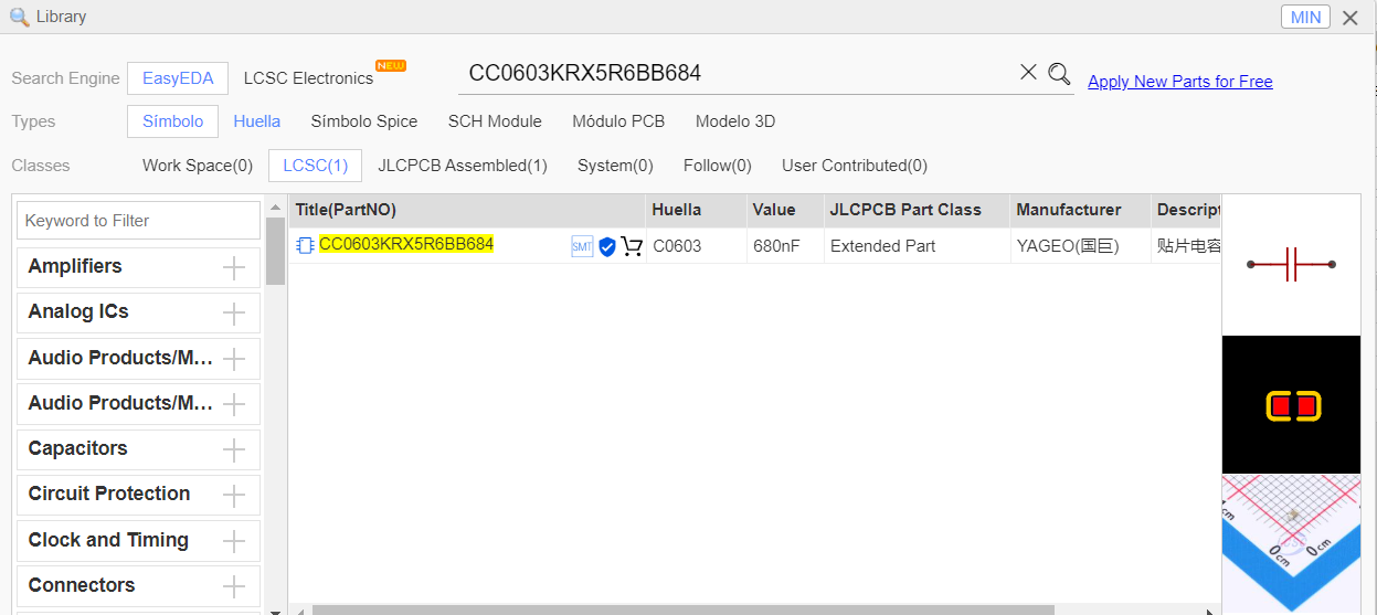
Hello,
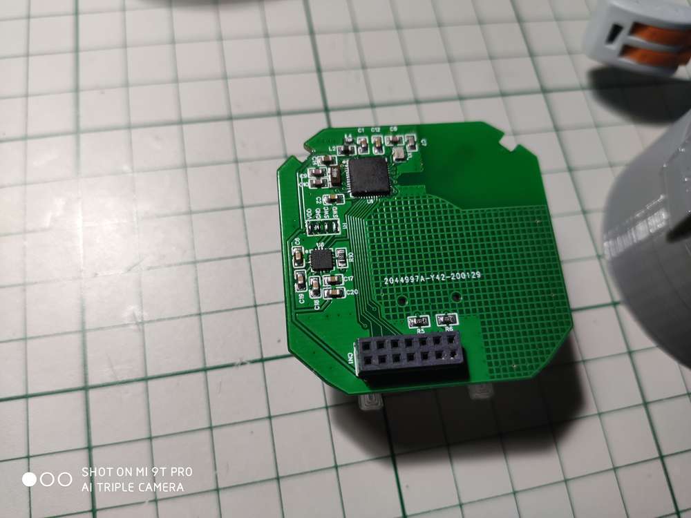
I looked for the manufaturer part of C10 in EasyEDA Library "CC0603KRX5R6BB684" and I noted that it describes a 680nF/10V capacitor, but in the schematic it is supposed to be 100nF/50V, (CC0603KRX7R9BB104), so which is correct?
Hello! It looks like you're interested in this conversation, but you don't have an account yet.
Getting fed up of having to scroll through the same posts each visit? When you register for an account, you'll always come back to exactly where you were before, and choose to be notified of new replies (either via email, or push notification). You'll also be able to save bookmarks and upvote posts to show your appreciation to other community members.
With your input, this post could be even better 💗
Register Login