Hi @nagelc, our CI pipeline is currently running cppcheck version 2.1. Could you let me know which version you're using on your end?
Posts
-
cppcheck old-style c cast -
What does --my-is-rfm69hw do?@nschurando Yes, the “C” in RFM69HCW (or RFM69CW) means “compatible”, indicating pin compatibility with older RFM modules such as the RFM12B.
-
Sleeping with RFM95 ?@Aymeric As @TheoL mentioned, the library automatically handles putting the radio to sleep when you call
sleep(). The functionstransportDisable()andtransportReinitialize()are internal to the library and not meant to be used directly.If you can share the serial/console output, we may be able to better understand what’s going on.
-
Forum Search not working?Search function restored
-
Code Garage to the rescue.@OldSurferDude The website should be back again.
-
MYSBootloader 1.3 pre-release & MYSController 1.0.0beta@luizrrocha Can you post your sketch and (if available) debug log here?
-
Instable ESP32 MQTT gateway with RFM69@electrik Probably this is PubSubClient-related. Please provide additional infos:
- ESP board definitions version
- MySensors version
- GW sketch
-
[RFM95] Ant Switch/TxRx switch pins@eiten A similar approach was used for a NRF5 +PA/LNA module: https://github.com/mysensors/MySensors/pull/1414/files#diff-7b958e4728831b83d2359a08827bcae1R64-R80
-
ATC and repeating nodes@eiten Would be helpful to see the debug logs (in rfm/sx verbose mode)
-
CubeCell reloaded: the SX126x hal drivers, please test@eiten Yep, already saw this one. Based on the heltec implementation, the sx-registers are mapped to specific memory regions of the mcu. Would be interesting to have here a complete ASR-specific documentation...
-
CubeCell reloaded: the SX126x hal drivers, please test@eiten Great job! Did you come across an "usable" ASR6501 datasheet - so far the information on this SoC is rather sparse?
-
[Solved] Arduino Nanos don't work as nodes@Avamander Can you upload both, the GW and node sketches from the working pair nanoGW/megaNode? Also, it would be helpful to see the full GW log from the non-working combination (nanoNode/megaGW) with
MY_DEBUG_VERBOSE_RF24enabled. If time allows, I'd like to reproduce and test your setup. -
Node to Node Communication via Gatreway@FullMetal said in Node to Node Communication via Gatreway: Please upload the debug logs for further troubleshooting.
-
[Solved] How to adjust MySBootloader files to compile other EN & CSN pins different channel and external 8MHz crystal@Joerideman Glad to hear you finally got FOTA working :+1: - generally speaking, you can do both, serial FW uploads and FOTA, however, switching from FOTA to serial updates or vice-versa, you may want to clear the FW checksum stored in the EEPROM as instructed above. If your sketches are rather large or for prototyping/dev, I'd advise you to use the optiboot bootloader as the serial uploads are faster and the optiboot bootloaders uses less flash storage...
-
[Solved] How to adjust MySBootloader files to compile other EN & CSN pins different channel and external 8MHz crystal@Joerideman That looks already much better!
For the sake of completeness, here is the modified MYSBootloader source code.
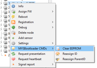
Try clearing the EEPROM and then re-assign the FW
-
[Solved] How to adjust MySBootloader files to compile other EN & CSN pins different channel and external 8MHz crystal@Joerideman You can ignore that warning (it is related to rm not being found).
Can you try this .hex file: CE=8, CSN=9, CLK=8MHz, BAUD=57600, RF24 channel=122: download file
Please post the log of the bootloader flashing process...
-
[Solved] How to adjust MySBootloader files to compile other EN & CSN pins different channel and external 8MHz crystal@Joerideman Thanks, I again had a quick look at your HW.h file and found the issue:
// set pin mode: MOSI,SCLK,CE,CSN = OUTPUT, MISO = INPUT (=> all on same port)
SPI_DDR = _BV(SPI_MOSI) | _BV(SPI_SCLK) | _BV(CE_PIN) | _BV(PB2) | ~_BV(SPI_MISO);
CSN_DDR = _BV(CSN_PIN);
SPI_DDR and CSN_DDR are both pointing at DDRB:
// SPI communication
#define SPI_PORT	PORTB	//
#define SPI_DDR		DDRB	//
and
#elif defined(SPI_PINS_CE8_CSN9)
	#define CSN_PORT	PORTB	// port for CSN
	#define CSN_DDR		DDRB	// DDR for CSN
	#define	CSN_PIN		PB1		// Arduino Pin 9 <-> Bit 1 of port B
Thus, setting CSN_DDR = _BV(CSN_PIN) you overwrite SPI_DDR. Comment out the second line and add _BV(CSN_PIN) to SPI_DDR:
// set pin mode: MOSI,SCLK,CE,CSN = OUTPUT, MISO = INPUT (=> all on same port) SPI_DDR = _BV(SPI_MOSI) | _BV(SPI_SCLK) | _BV(CE_PIN) | _BV(PB2) | _BV(CSN_PIN); //CSN_DDR = _BV(CSN_PIN); -
Node to Node Communication via Gatreway@FullMetal Please post a full debug log of both nodes showing the observed behaviour.
-
[Solved] How to adjust MySBootloader files to compile other EN & CSN pins different channel and external 8MHz crystal@Joerideman Yeah, I assume something is wrong with the bootloader configuration. Can you zip and upload all bootloader files (or the entire folder) you are using with all the settings and modifications you did?
-
[Solved] How to adjust MySBootloader files to compile other EN & CSN pins different channel and external 8MHz crystal@Joerideman The bootloader doesn't generate serial debug output, would be helpful to see the GW debug log