In wall light switch node - Custom PCB
-
@samuel235 said:
Both of the boards have CTS shorted to GND. I didn't explain it correctly, i meant that if i use GND (on the USB adapter) -> GND on board, nothing happens. But if i do CTS (on the USB adapter) -> GND or CTS on board, it works for the APM.
Sorry, I still don't get it. Don't you always connect all 6 pins?
Now i have some progress. I made the fundamental error of not powering the board with the battery while it was connect to FTDI.
Great, but you should not need a battery if you have power from the FTDI-adapter and don't have any big power consumers or shorts on the board. Do you use 5 or 3.3V ? Have you measured the current (e.g. from a battery)?
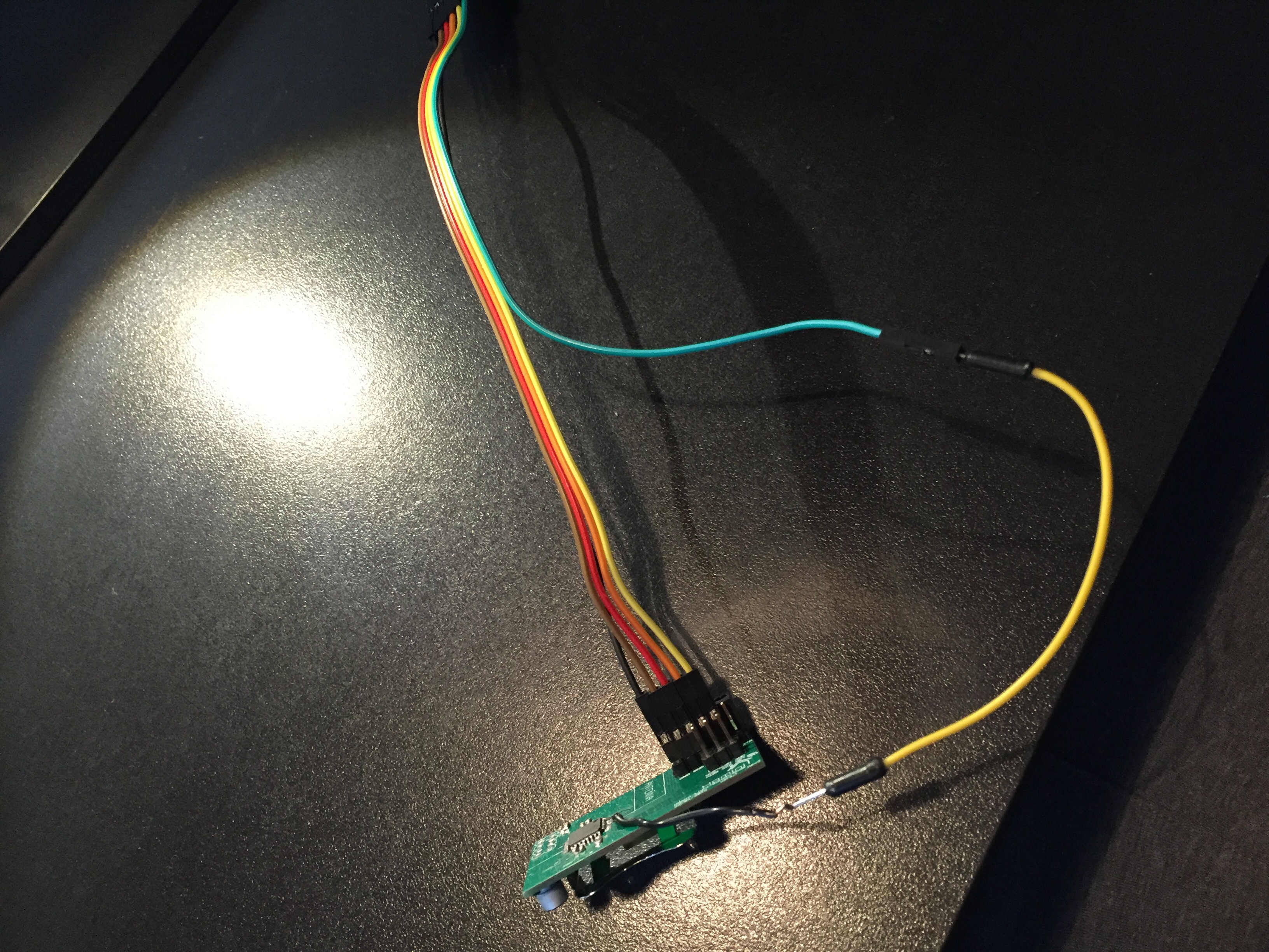
@m26872 - Both of the adapters that i purchased only came with 5 wires in a ribbon cable fashion, and me being mr gullible decided to assume that it only needed the 5. I just assumed that i only need to connect GND OR CTS. I'm now assuming that i need to connect both of them as they don't short together on the adapter itself? I have watched numerous videos on FTDI and ISP to troubleshoot this and I can honestly admit that i didn't realise if any of them had used 6 connections :(
I did at one point test the current, i can't remember exactly what it was. Give me an hour and I will be able to test that :) - I'm using 3.3v for the VCC line, my adapter is set to 3.3v too. Does it matter what the current is or would you be checking to just see if there is any current at all? I have tested the voltages when i'm hooked up to the serial connection just to let you know, and they were fine across all of the vcc connections on the board, so there is no connections missing and the uC is definably receiving power :)
-
So i have just dropped my multimeter over the coin cell and various other positions on the board, it would seem that there isn't much of a current change anywhere across the board. It reads 2.6mA across the board. This shows that there isn't really any current draw across the board and therefor like @m26872 mentioned in the previous post, there is no reason to why it shouldn't work being powered from the serial adapter.
When i have the board connected through the serial adapter without the battery, the current is the same across the board, the reset pin is receiving the 3v to keep it high and i get an error of:
avrdude: stk500_getparm(): (a) protocol error, expect=0x14, resp=0xfc

avrdude: stk500_getparm(): (a) protocol error, expect=0x14, resp=0xfc

avrdude: arduino_read_sig_bytes(): (a) protocol error, expect=0x10, resp=0xfc
avrdude: error reading signature data for part "ATmega328P", rc=-3
Problem uploading to board.  See http://www.arduino.cc/en/Guide/Troubleshooting#upload for suggestions.
avrdude: error reading signature data, rc=-1
I don't think there errors are very helpful as they keep changing every time i try to upload it without touching the board. I think its just having general issues with getting a transmit signal. I can still view the serial monitor perfectly fine which to me indicates that i have the Rx and the Tx line correct for a start. Am I correct in assuming this?
What is your general thoughts, would you think it has anything to do with the reset procedure or do you feel there is an issue elsewhere on the board/power?
EDIT: I measured the current incorrectly, changed the figure in this post to reflect the correct measurement.
-
I can also confirm that my RESET pin is high with the same voltage as the coin cell is providing so there is no issue from the start of the process, the only thing I'm wondering is if the DTR pin is pulling the pin low when needed. This process would be much easier to see if i had an oscilloscope.
-
I can now rule out my previous thoughts of the capacitor on the DTR line being too far away from the FTDI connector, i just moved its placement and it doesn't change a thing. Still getting the protocol error.
-
I can now rule out my previous thoughts of the capacitor on the DTR line being too far away from the FTDI connector, i just moved its placement and it doesn't change a thing. Still getting the protocol error.
@samuel235 I looked again at your board and saw that your DTR trace was routed very near Rx. Did your "move" of C7 had it's own wire from serial adapter, i.e. bypassed and unconnected to DTR trace on board?
I also pressume you've double checked value and functionality of C7. -
@samuel235 I looked again at your board and saw that your DTR trace was routed very near Rx. Did your "move" of C7 had it's own wire from serial adapter, i.e. bypassed and unconnected to DTR trace on board?
I also pressume you've double checked value and functionality of C7.I completely moved C7 and infact i attached it to the under side of the DTR pin on the FTDI header, then ran a wire to the pad that C7 WAS attached to (the uC side). I made sure it was not shorting on anything else in its vicinity.
I do understand the functionality and the value needed for this cap. The need for this cap is to essensially pull the RESET line low for a split second by discharging the cap and then the vcc line with the pullup resistor charges the cap back to full then pulls the reset pin high. This process then tell the uC to restart itself.
The only thing left for me to try is increasing the size of that cap. I have a 4.7uF cap in my inventory that i will attempt to change out. But i have read that everyone uses a 0.1uF and its very very unlikely that it needs to be higher. My case might just be that 0.1% that does.
-
I completely moved C7 and infact i attached it to the under side of the DTR pin on the FTDI header, then ran a wire to the pad that C7 WAS attached to (the uC side). I made sure it was not shorting on anything else in its vicinity.
I do understand the functionality and the value needed for this cap. The need for this cap is to essensially pull the RESET line low for a split second by discharging the cap and then the vcc line with the pullup resistor charges the cap back to full then pulls the reset pin high. This process then tell the uC to restart itself.
The only thing left for me to try is increasing the size of that cap. I have a 4.7uF cap in my inventory that i will attempt to change out. But i have read that everyone uses a 0.1uF and its very very unlikely that it needs to be higher. My case might just be that 0.1% that does.
@samuel235 If you mean the Ftdi header on the board, then it was still connected to that trace. Try bypass it completely and connect straigth from your serial adapter to cap to resetpin.
-
@samuel235 If you mean the Ftdi header on the board, then it was still connected to that trace. Try bypass it completely and connect straigth from your serial adapter to cap to resetpin.
@m26872 Of course it would, silly me. I have now ammended that and still nothing. I'm about to swap out that cap for a 4.7 to see if that does it. This is how i have it setup to test what you pointed out:
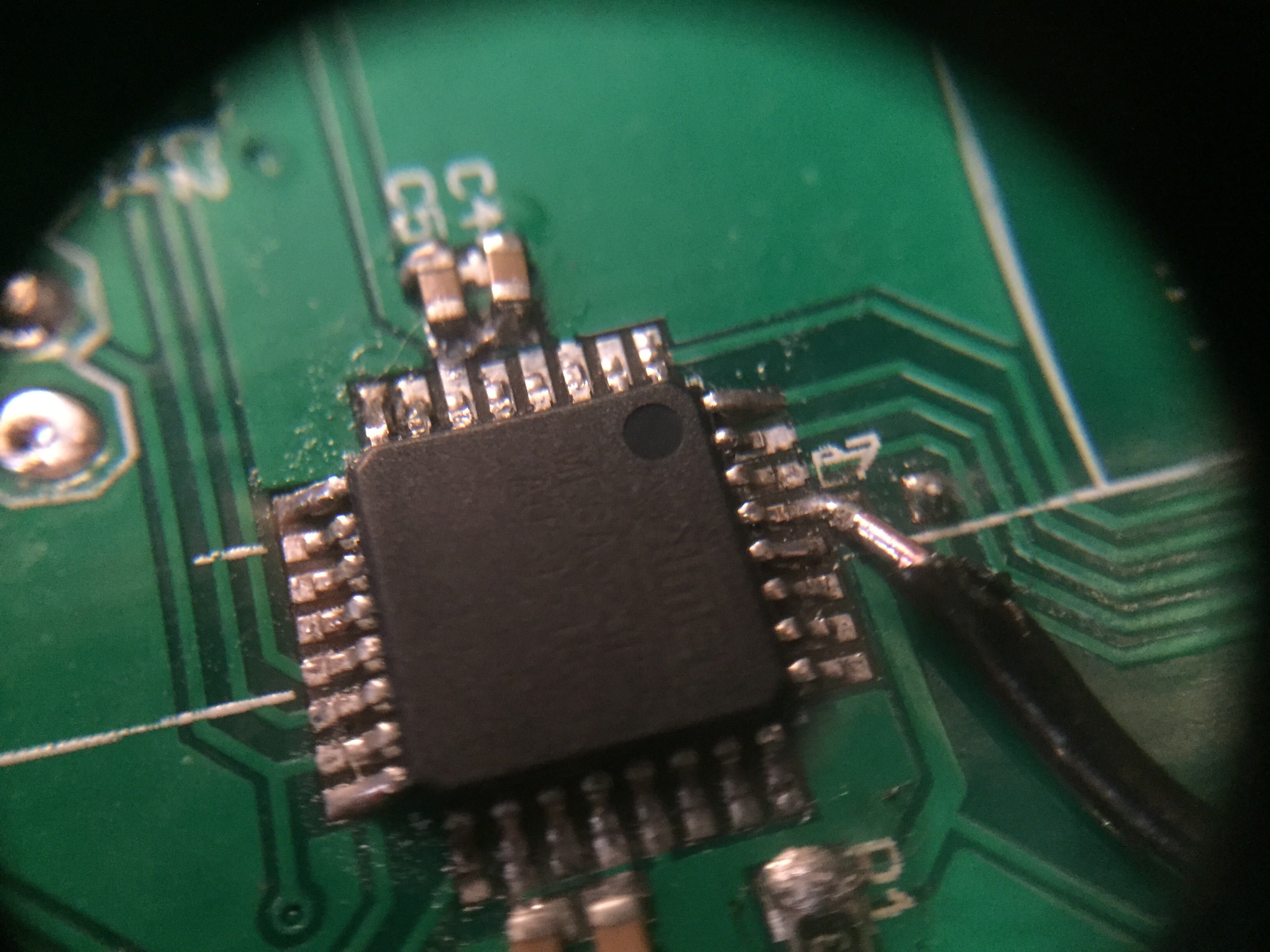
Photographing my board under x25 magnification makes it look very amateurish and dirty :(
-
Does anyone have another bootloader that works with the atmega328p-au clocked using the internal oscillator at 8MHz? I just want to double check it isnt my bootloader playing up with the clocking speeds. That or a boards.txt section for this setup. I will edit my own later but i would just like to double/triple check it with one that has been made from someone other than myself to rule out any silly errors.
-
Scrap that idea, my Arduino Pro Mini is working perfect with the exact same fuse settings, boards.txt entry and sketch.
-
So after several discussions with some atmel information being thrown around over the arduino forums i have came to the point where i have now found out that using the internal oscillator will not always allow serial connections/uploads to work properly. So, at the moment to test this, i burnt the sketch using 'upload via programmer' and then unplugged the board and re-connected using FTDI connections. I then opened the serial monitor and its working perfect. Next up is to figure out some information regarding crystals. With the whole board running on a coin cell my main point was to have the power consumption as low as possible. Could anyone give me some information or websites regarding oscillators, i would like to know if they use any extra power consumption compared to using the internal crystal of the atmega328p-au.
I have two options for this board where i would like to take it;
- Add an external crystal and allow users to upload via FTDI without having to touch the ISP connection/burning a new bootloader.
- Keep the internal crystal in use, and instruct the users to upload via ISP with the programmer and then debug using serial connection.
-
I'm now sitting with two of these boards in front of me giving me an "Starting sensor (1.6.0-beta), Radio init failed. Check wiring.". As i already have experienced this, i do know that 9/10 times this is hardware related. Normally incorrect wiring. Time to troubleshoot this for the second day. I'm pretty sure that i have no shorts on the board, the only thing that i can think it could be is a broken radio, but with the two doing this i'm a little skeptical about that.
-
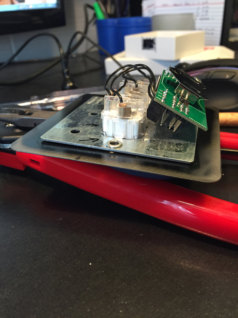
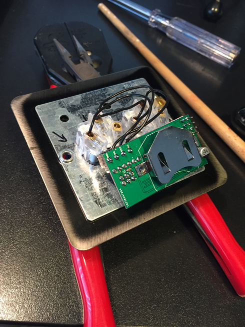
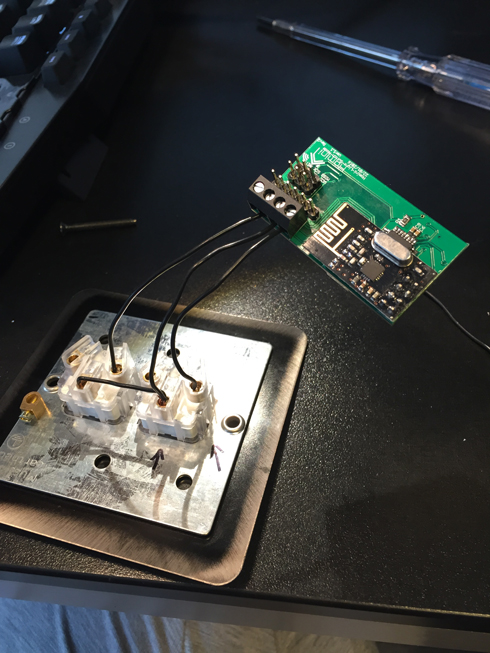
So here we have it guys, Revision 2 is now complete, tested and working perfectly! Its been a grueling process but so rewarding. I plan on making a few tiny little changes, including some headers/jumpers to allow ISP uploads while the radio is attached and pull-up resistors to the switch lines. I will get these all ironed out in the next few days and get the designs sent off to get the final boards manufactured. However, I don't feel that there is a great rush for this last board as the upgrades are very minor ones that won't effect its usability right now. The files on the original post are all up to date and relevant including the schematic. I'm yet to test the current draw, I'm trusting that it is sleeping in between the switch toggles, would this be tested via the current draw, if so where should it be measured to confirm this?
Here are a few photographs of the final board attached to a switch plate:
-
Hi,
I'm trying to order this PCB pre-assembled from itead.cc, but it requires Gerber and BOM files, none of which are found in the Eagle files zip...
Any idea how can I get this PCB pre-assembled?
-
Hi,
I'm trying to order this PCB pre-assembled from itead.cc, but it requires Gerber and BOM files, none of which are found in the Eagle files zip...
Any idea how can I get this PCB pre-assembled?
I'm affraid i don't have this board set up with any distributor for pre-assembly sales. The only option to get this board pre made would be for me (or anyone else willing to build the board) to build the board for you then mail to you. I can supply you with the gerber files and everything needed to purchase the board and a BOM then you can build the board yourself if thats possible.
MySensors 2.1.1
Controller - OpenHAB (Virtual Machine)
Gateway - Arduino Mega MQTT Gateway W5100 -
I'm affraid i don't have this board set up with any distributor for pre-assembly sales. The only option to get this board pre made would be for me (or anyone else willing to build the board) to build the board for you then mail to you. I can supply you with the gerber files and everything needed to purchase the board and a BOM then you can build the board yourself if thats possible.
@samuel235
That is a shame, this looks like exactly what I was looking for, though the assembly is way over my head. This is why I was hoping to get it pre-assembled...I can handle the basic soldering of a capacitor or varistor, but not their miniature versions, not to mention the atmega chip...
-
I'm affraid i don't have this board set up with any distributor for pre-assembly sales. The only option to get this board pre made would be for me (or anyone else willing to build the board) to build the board for you then mail to you. I can supply you with the gerber files and everything needed to purchase the board and a BOM then you can build the board yourself if thats possible.
@samuel235 said:
I'm affraid i don't have this board set up with any distributor for pre-assembly sales. The only option to get this board pre made would be for me (or anyone else willing to build the board) to build the board for you then mail to you. I can supply you with the gerber files and everything needed to purchase the board and a BOM then you can build the board yourself if thats possible.
I'd appreciate the gerber and BOM files, though!
Could you add a link to them in the first post? -
@samuel235 said:
I'm affraid i don't have this board set up with any distributor for pre-assembly sales. The only option to get this board pre made would be for me (or anyone else willing to build the board) to build the board for you then mail to you. I can supply you with the gerber files and everything needed to purchase the board and a BOM then you can build the board yourself if thats possible.
I'd appreciate the gerber and BOM files, though!
Could you add a link to them in the first post?@Sefi-Ninio - Soon as i get home from work tonight i will get that sorted for you. However i do advise you waiting for revision 3 to come out as currently a new sketch/program can't be uploaded to the uC while the radio is attached.
MySensors 2.1.1
Controller - OpenHAB (Virtual Machine)
Gateway - Arduino Mega MQTT Gateway W5100 -
@Sefi-Ninio - Soon as i get home from work tonight i will get that sorted for you. However i do advise you waiting for revision 3 to come out as currently a new sketch/program can't be uploaded to the uC while the radio is attached.
@samuel235 said:
@Sefi-Ninio - Soon as i get home from work tonight i will get that sorted for you. However i do advise you waiting for revision 3 to come out as currently a new sketch/program can't be uploaded to the uC while the radio is attached.
Thanks!
When do you think rev. 3 will come out and tested? -
Depending on my full-time job workload, I'm hoping to have the designs completed and sent off for manufacturing by sunday, but then we face the 3 week wait for the shipping, and then the testing +/- a week for constant testing measures.
Hello! It looks like you're interested in this conversation, but you don't have an account yet.
Getting fed up of having to scroll through the same posts each visit? When you register for an account, you'll always come back to exactly where you were before, and choose to be notified of new replies (either via email, or push notification). You'll also be able to save bookmarks and upvote posts to show your appreciation to other community members.
With your input, this post could be even better 💗
Register Login