Novice requesting PCB review and advice for a window / door sensor
-
Quick links to posts with major updates
- 14 Dec 2018
First revision with a much more compact design and an Attiny84 variant - 7 Jan 2019
Second revision with more functionality, but without increasing the PCB size - 25 Mar 2019
PCBs arrived, ATmeg328P-based device is built and fully working
Original Post
Hi there,
I’ve started discovering the world of electronics through Arduino about three month ago and decided recently to get a little bit more serious about it. I’m designing my first custom PCB which should be used as a base for a little door / window sensor with an Atmega328P as its heart and the MySensors library as its soul.
I’m hopeful to find some knowledgeable guys over here, who could have a quick look at my design, point out flaws, give advice. That’d be awesome!
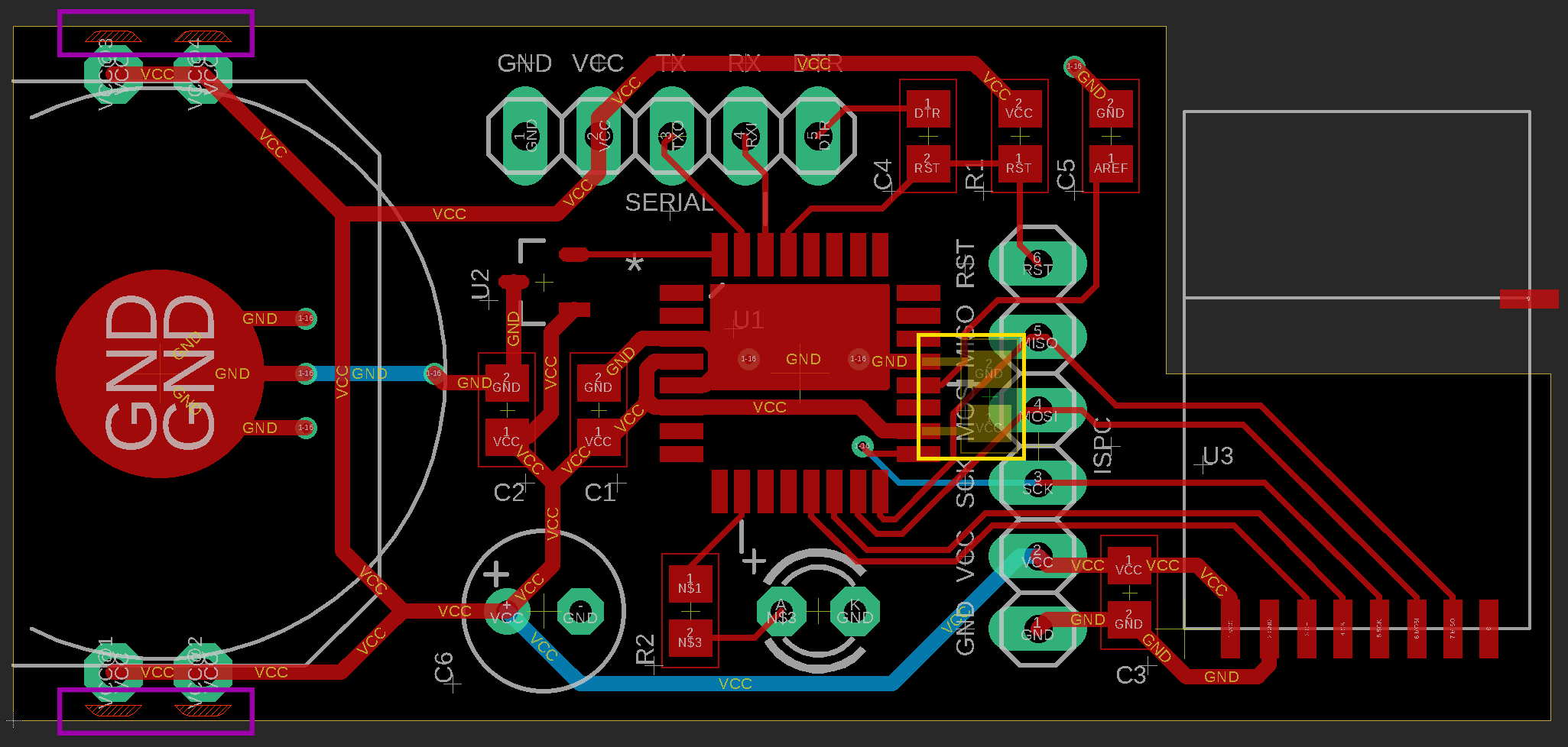
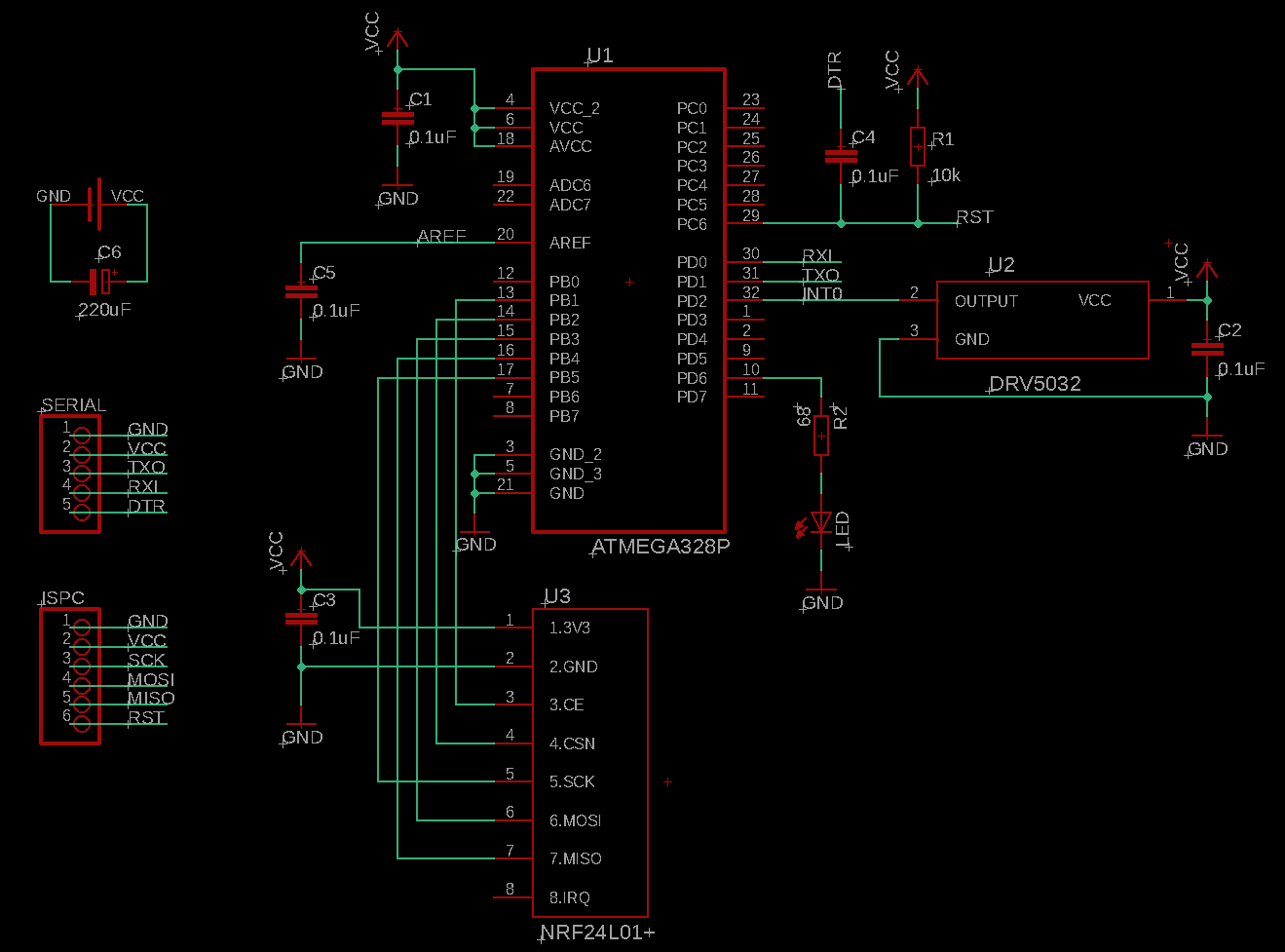
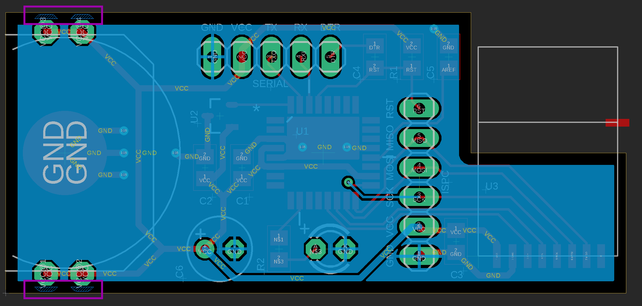
Before we go into the details, let’s have a quick look at the schematic and layout:
Schematic

Top layer
Bottom layer

The GND on the top layer as well as all VCC routes are 20 mil wide, all other signals are 8 mil wide. Clearances in DRC are 8 mil for everything. The bottom layer has a large ground fill, which I tried to keep as clean as possible.
Part List
- U1: Atmega328P-AU
- U2: DRV5032FB
- U3: NRF24L01+ (SMD module)
- C1, C2, C3, C4, C5: 100 nF Y5V MLCC
- C6: 220 µF 6.3V electrolytic
- R1: 10k Ω
- R2: 68 Ω
- 3V CR2032
Concept and functionality
By designing this board I had three main aspects in mind:
- Should be able to run for (many) years off a single coin cell
- Keep it as small as possible … (currently ~ 2x the size of an Arduino Pro Mini)
- … but still solderable by hand (no parts smaller than 0805)
The circuit goes into power-down mode by default, where it should consume ~ 2 µA (plus whatever leakage current might be introduced by the capacitors, I expect no more than 1-2 µA extra based on my own tests) - I measured ~ 1.5 µA on prototypes I’m currently running, which feature a mechanical reed switch instead of a digital hall effect sensor. When the hall effect sensor detects a change (window opened or closed), it wakes the Atmega via interrupt on INT0. The MCU then sends the current state along with the voltage level over the radio module to the master node and goes back into power-down mode.
Speaking of the hall effect sensor: the DRV5032 is a ultra-low power sensor from TI, which can be powered between 1.65 and 5.5V. The FB-variant is omni-polar and particularly economical, as it operates at only 5 Hz and has a push-pull output which means that no external pull-up resistor is needed, bringing its current consumption down to an average of 0.7 µA or less at 3V and below.
You are almost certainly already familiar with the good old Atmega328P and the NRF24L01+ radios, so I won’t waste no words on them.
Now that you have a basic idea of my thoughts and goals, let’s get to the fun part:
My questions / concerns / uncertainties:
-
DRC check yields zero errors, except for the through hole mounting points of the battery holder (marked in purple on the layout screenshots), which are quite close to the edge of the board. That should pose no problem, should it?
-
Regarding ceramic capacitor positioning and their capacity: I’ve tried to get each MLCC as close to the corresponding GND and VCC pins of the components they belong to, so that they create their own little "current loop". The sensor, MCU and radio each get a single 100 nF capacitor. Is that sufficient?
Is it advisable to add a second 100 nF cap to the AVCC / GND pair on the right side of the MCU (marked in yellow)?
[EDIT: The AVR Hardware Design Guide clearly states "For devices with multiple pairs of power and ground pins, it is essential that there is a decoupling capacitor for every pair of pins" and "To improve the accuracy of the ADC, the analog supply voltage must be decoupled separately, similar to the digital supply voltage", but I see that many people don't do so and by trying to keep it simple, I thought it is worth the question anyway.]The 220 µF electrolytic cap should protect the coin cell from sudden current spikes when the radio is in transmission mode and should be able to deliver most of the current during this time, so I don’t think the radio needs another ~ 10 µF MLCC near it, does it?
-
I would like to make use of the FOTA functionality of the MySensors library - not because I expect to change the code frequently, but just in case, for convenience - but I didn’t have time to mess with this yet. So the question is, if I need to be able to upload the actual sketch physically / wired for the first time - like with ArduinoOTA for the ESP8266, before you can use the wireless upload? If not, I’d gladly remove the serial header entirely.
I might also remove the LED, as I probably won’t use it in the final build to save power - I’m currently using them on the prototypes to see when and for how long they wake up. With the saved space I might either try to make this thing even smaller or a little more versatile by adding additional headers for I2C / SPI instead.
Thanks for your attention and patience if you actually read everything! :)
- 14 Dec 2018
-
Quick links to posts with major updates
- 14 Dec 2018
First revision with a much more compact design and an Attiny84 variant - 7 Jan 2019
Second revision with more functionality, but without increasing the PCB size - 25 Mar 2019
PCBs arrived, ATmeg328P-based device is built and fully working
Original Post
Hi there,
I’ve started discovering the world of electronics through Arduino about three month ago and decided recently to get a little bit more serious about it. I’m designing my first custom PCB which should be used as a base for a little door / window sensor with an Atmega328P as its heart and the MySensors library as its soul.
I’m hopeful to find some knowledgeable guys over here, who could have a quick look at my design, point out flaws, give advice. That’d be awesome!
Before we go into the details, let’s have a quick look at the schematic and layout:
Schematic

Top layer

Bottom layer

The GND on the top layer as well as all VCC routes are 20 mil wide, all other signals are 8 mil wide. Clearances in DRC are 8 mil for everything. The bottom layer has a large ground fill, which I tried to keep as clean as possible.
Part List
- U1: Atmega328P-AU
- U2: DRV5032FB
- U3: NRF24L01+ (SMD module)
- C1, C2, C3, C4, C5: 100 nF Y5V MLCC
- C6: 220 µF 6.3V electrolytic
- R1: 10k Ω
- R2: 68 Ω
- 3V CR2032
Concept and functionality
By designing this board I had three main aspects in mind:
- Should be able to run for (many) years off a single coin cell
- Keep it as small as possible … (currently ~ 2x the size of an Arduino Pro Mini)
- … but still solderable by hand (no parts smaller than 0805)
The circuit goes into power-down mode by default, where it should consume ~ 2 µA (plus whatever leakage current might be introduced by the capacitors, I expect no more than 1-2 µA extra based on my own tests) - I measured ~ 1.5 µA on prototypes I’m currently running, which feature a mechanical reed switch instead of a digital hall effect sensor. When the hall effect sensor detects a change (window opened or closed), it wakes the Atmega via interrupt on INT0. The MCU then sends the current state along with the voltage level over the radio module to the master node and goes back into power-down mode.
Speaking of the hall effect sensor: the DRV5032 is a ultra-low power sensor from TI, which can be powered between 1.65 and 5.5V. The FB-variant is omni-polar and particularly economical, as it operates at only 5 Hz and has a push-pull output which means that no external pull-up resistor is needed, bringing its current consumption down to an average of 0.7 µA or less at 3V and below.
You are almost certainly already familiar with the good old Atmega328P and the NRF24L01+ radios, so I won’t waste no words on them.
Now that you have a basic idea of my thoughts and goals, let’s get to the fun part:
My questions / concerns / uncertainties:
-
DRC check yields zero errors, except for the through hole mounting points of the battery holder (marked in purple on the layout screenshots), which are quite close to the edge of the board. That should pose no problem, should it?
-
Regarding ceramic capacitor positioning and their capacity: I’ve tried to get each MLCC as close to the corresponding GND and VCC pins of the components they belong to, so that they create their own little "current loop". The sensor, MCU and radio each get a single 100 nF capacitor. Is that sufficient?
Is it advisable to add a second 100 nF cap to the AVCC / GND pair on the right side of the MCU (marked in yellow)?
[EDIT: The AVR Hardware Design Guide clearly states "For devices with multiple pairs of power and ground pins, it is essential that there is a decoupling capacitor for every pair of pins" and "To improve the accuracy of the ADC, the analog supply voltage must be decoupled separately, similar to the digital supply voltage", but I see that many people don't do so and by trying to keep it simple, I thought it is worth the question anyway.]The 220 µF electrolytic cap should protect the coin cell from sudden current spikes when the radio is in transmission mode and should be able to deliver most of the current during this time, so I don’t think the radio needs another ~ 10 µF MLCC near it, does it?
-
I would like to make use of the FOTA functionality of the MySensors library - not because I expect to change the code frequently, but just in case, for convenience - but I didn’t have time to mess with this yet. So the question is, if I need to be able to upload the actual sketch physically / wired for the first time - like with ArduinoOTA for the ESP8266, before you can use the wireless upload? If not, I’d gladly remove the serial header entirely.
I might also remove the LED, as I probably won’t use it in the final build to save power - I’m currently using them on the prototypes to see when and for how long they wake up. With the saved space I might either try to make this thing even smaller or a little more versatile by adding additional headers for I2C / SPI instead.
Thanks for your attention and patience if you actually read everything! :)
@bearwithbeard I don’t know much about pcb design but the serial header could be useful when debugging/troubleshooting so personally I would prefer that at least the tx pin is available. Some people have used pogo pin connectors to save space.
- 14 Dec 2018
-
Oh, answers! Thank you guys, appreciated! I've changed the layout quite a bit since I started this thread. I've also already ordered PCBs for them. But more on that later, let me get to your messages first:
@huex said in Novice requesting PCB review and advice for a window / door sensor:
looks good ,
but sot23 maybe needs to be a specific direction. or TO-92s?Uhm, you are talking about U2, the hall effect switch? Since it has two pins on one and only one pin on the other side of the package, I don't think it can be soldered the wrong way around. :thinking_face:
Or are you talking about the orientation in relation the the magnetic field? As far as I understand the data sheet, it doesn't matter if the sensor is mounted horizontally or vertically. The only requirement seems to be that the magnetic field is perpendicular to the top of the package - and its strength of course.@dbemowsk said in Novice requesting PCB review and advice for a window / door sensor:
I thought it was more common for the ISP header to be 2 rows of 3 pins instead of a straight 6 pins? Not that you can't make that work.
Yes, you are correct, a 2x3 header would be preferable, so that you could simply plug your standard adapter on it. The reason for the single row in the design was to save horizontal space and it also allowed a much cleaner routing of the signals to the NRF24.
@mfalkvidd said in Novice requesting PCB review and advice for a window / door sensor:
@bearwithbeard I don’t know much about pcb design but the serial header could be useful when debugging/troubleshooting so personally I would prefer that at least the tx pin is available. Some people have used pogo pin connectors to save space.
I understand your point. But IMHO debugging and troubleshooting should take place on a breadboarded version before switching to a rather permanent solution like this.
I will have a look at those pogo pins, thank you!
@flopp said in Novice requesting PCB review and advice for a window / door sensor:
U1, you have a lot of GND-area underneath the atmega328, it may be possible that a pin close to this area will touch the area and you will get a short circuit between a pin and area.
The ground area on the top PCB layer underneath the MCU would be covered by a soldermask. So, as far as I understand, it shouldn't be possible to short a pin with this area, as long as the mask isn't scratched off or improperly applied by the manufacturer. Am I wrong?
The updated layout
As I says earlier, I made some changes to this project. Here's a quick summary:
I've designed an additional variant with an Attiny84
I'm waiting for parts to arrive to test the setup with the Attiny, but I'm confident it will work. If it will, it reduces the total cost per device by ~1.2 Euro / 1.35 USD, allows for a ~7mm narrower package and makes it easier to solder.
I've decided to exchange the 220 µF electrolytic cap for a 10 - 22 µF MLCC.
This should significantly reduce potential battery capacity losses through leakage current a "bad" electrolytic cap could introduce. It should also be sufficient to cushion the initial current spike when the NRF24 enters transmission mode and will also step in faster as the electrolytic cap would be able to.
Status LED and serial header removed
I simply saw no need for those parts anymore. Using the LED as a “I noticed that you closed / opened the window”-status indicator would add another 10 - 20 mA for a few ms and - let’s be honest - nobody would want to stare at the sensor whenever they open or close a window to see if it detected it, they would simply expect it to work. Letting it light up periodically in case of a fault or as a low battery indicator, drains to much battery juice and would better be handled in the backend / by the server, I think.
Keeping a separate TX pin, as @mfalkvidd mentioned, might be useful along with a jumper to optionally enable debugging output, I guess. I might add that in a later revision. Makes more and more sense the longer I think about it.I quickly made some screenshots of the top layers of each version:
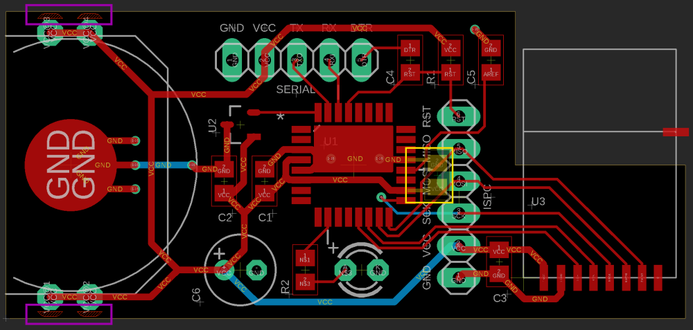
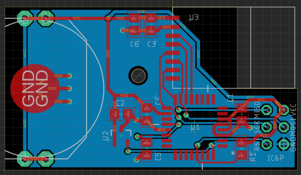
With Atmega328P
With Attiny84
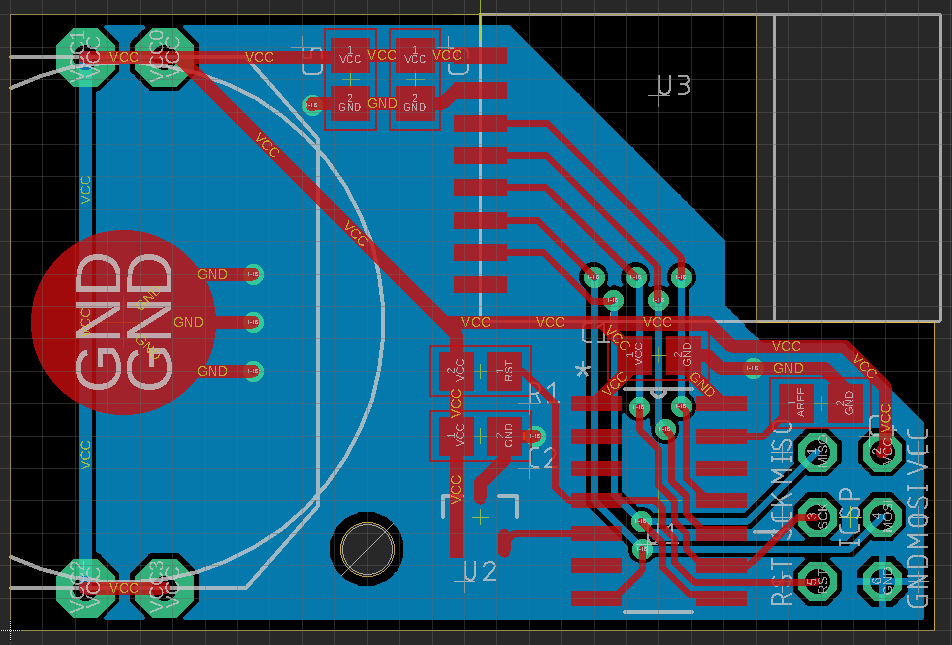
With all those changes, I was able to shrink the PCB to roughly the size of two CR2032 coin cell holders: 24 x 43 mm for the Atmega variant and 24 x 36 mm for the Attiny variant. Pretty happy with that.
Your comments and opinions are still appreciated!
-
Quick links to posts with major updates
- 14 Dec 2018
First revision with a much more compact design and an Attiny84 variant - 7 Jan 2019
Second revision with more functionality, but without increasing the PCB size - 25 Mar 2019
PCBs arrived, ATmeg328P-based device is built and fully working
Original Post
Hi there,
I’ve started discovering the world of electronics through Arduino about three month ago and decided recently to get a little bit more serious about it. I’m designing my first custom PCB which should be used as a base for a little door / window sensor with an Atmega328P as its heart and the MySensors library as its soul.
I’m hopeful to find some knowledgeable guys over here, who could have a quick look at my design, point out flaws, give advice. That’d be awesome!
Before we go into the details, let’s have a quick look at the schematic and layout:
Schematic

Top layer

Bottom layer

The GND on the top layer as well as all VCC routes are 20 mil wide, all other signals are 8 mil wide. Clearances in DRC are 8 mil for everything. The bottom layer has a large ground fill, which I tried to keep as clean as possible.
Part List
- U1: Atmega328P-AU
- U2: DRV5032FB
- U3: NRF24L01+ (SMD module)
- C1, C2, C3, C4, C5: 100 nF Y5V MLCC
- C6: 220 µF 6.3V electrolytic
- R1: 10k Ω
- R2: 68 Ω
- 3V CR2032
Concept and functionality
By designing this board I had three main aspects in mind:
- Should be able to run for (many) years off a single coin cell
- Keep it as small as possible … (currently ~ 2x the size of an Arduino Pro Mini)
- … but still solderable by hand (no parts smaller than 0805)
The circuit goes into power-down mode by default, where it should consume ~ 2 µA (plus whatever leakage current might be introduced by the capacitors, I expect no more than 1-2 µA extra based on my own tests) - I measured ~ 1.5 µA on prototypes I’m currently running, which feature a mechanical reed switch instead of a digital hall effect sensor. When the hall effect sensor detects a change (window opened or closed), it wakes the Atmega via interrupt on INT0. The MCU then sends the current state along with the voltage level over the radio module to the master node and goes back into power-down mode.
Speaking of the hall effect sensor: the DRV5032 is a ultra-low power sensor from TI, which can be powered between 1.65 and 5.5V. The FB-variant is omni-polar and particularly economical, as it operates at only 5 Hz and has a push-pull output which means that no external pull-up resistor is needed, bringing its current consumption down to an average of 0.7 µA or less at 3V and below.
You are almost certainly already familiar with the good old Atmega328P and the NRF24L01+ radios, so I won’t waste no words on them.
Now that you have a basic idea of my thoughts and goals, let’s get to the fun part:
My questions / concerns / uncertainties:
-
DRC check yields zero errors, except for the through hole mounting points of the battery holder (marked in purple on the layout screenshots), which are quite close to the edge of the board. That should pose no problem, should it?
-
Regarding ceramic capacitor positioning and their capacity: I’ve tried to get each MLCC as close to the corresponding GND and VCC pins of the components they belong to, so that they create their own little "current loop". The sensor, MCU and radio each get a single 100 nF capacitor. Is that sufficient?
Is it advisable to add a second 100 nF cap to the AVCC / GND pair on the right side of the MCU (marked in yellow)?
[EDIT: The AVR Hardware Design Guide clearly states "For devices with multiple pairs of power and ground pins, it is essential that there is a decoupling capacitor for every pair of pins" and "To improve the accuracy of the ADC, the analog supply voltage must be decoupled separately, similar to the digital supply voltage", but I see that many people don't do so and by trying to keep it simple, I thought it is worth the question anyway.]The 220 µF electrolytic cap should protect the coin cell from sudden current spikes when the radio is in transmission mode and should be able to deliver most of the current during this time, so I don’t think the radio needs another ~ 10 µF MLCC near it, does it?
-
I would like to make use of the FOTA functionality of the MySensors library - not because I expect to change the code frequently, but just in case, for convenience - but I didn’t have time to mess with this yet. So the question is, if I need to be able to upload the actual sketch physically / wired for the first time - like with ArduinoOTA for the ESP8266, before you can use the wireless upload? If not, I’d gladly remove the serial header entirely.
I might also remove the LED, as I probably won’t use it in the final build to save power - I’m currently using them on the prototypes to see when and for how long they wake up. With the saved space I might either try to make this thing even smaller or a little more versatile by adding additional headers for I2C / SPI instead.
Thanks for your attention and patience if you actually read everything! :)
Hello, and congratulations for a first PCB you seem to have carefully thought it out.
@bearwithbeard said in Novice requesting PCB review and advice for a window / door sensor:
DRC check yields zero errors, except for the through hole mounting points of the battery holder (marked in purple on the layout screenshots), which are quite close to the edge of the board. That should pose no problem, should it?
It will depends of the capabilities of the PCB maker, you should adjust the rules file used for DRC accordingly.
Regarding ceramic capacitor positioning and their capacity: I’ve tried to get each MLCC as close to the corresponding GND and VCC pins of the components they belong to, so that they create their own little "current loop". The sensor, MCU and radio each get a single 100 nF capacitor. Is that sufficient?
Is it advisable to add a second 100 nF cap to the AVCC / GND pair on the right side of the MCU (marked in yellow)?I would add one, it's not a lot of work and it will give you more stable power source for ADC when you measure battery voltage.
The 220 µF electrolytic cap should protect the coin cell from sudden current spikes when the radio is in transmission mode and should be able to deliver most of the current during this time, so I don’t think the radio needs another ~ 10 µF MLCC near it, does it?
The one close to the radio will help for the noise and it can be necessary for the current spikes depending on the distance with the main capacitor.
Regarding your last post with updates your reserve cap is too small, with around 3V on the battery pin you need to derate the capacity by around 50%, there were many posts related to button cell on the forum, and advice from reputable sources was to use around 100uF MLCC.I would like to make use of the FOTA functionality of the MySensors library - not because I expect to change the code frequently, but just in case, for convenience - but I didn’t have time to mess with this yet. So the question is, if I need to be able to upload the actual sketch physically / wired for the first time - like with ArduinoOTA for the ESP8266, before you can use the wireless upload? If not, I’d gladly remove the serial header entirely.
You need to burn a specific bootloader to manage FOTA, so you need headers. As said before, it's also useful for debugging with serial output, make tests like power consumption depending of different programming options, etc.
Regarding LED you don't need 10-20mA, if you use a small SMD led it can go well below 1mA and still produce a decent amount of light, I use around 200uA with a 0603 green led of one of my boards and the light is pretty bright.
Led can also be used to warn of errors, for example different blink count/duration based on an error during initialization, like when it can't find parent etcLast thing, I would avoid traces and components next to the antenna. The ICSP header is in a very bad position imho. Your bottom layer seems nearly empty, I would move the battery holder to the bottom layer and translate all components to the left so that ICSP header is no more next to the antenna area.
I would also add a ground pour on top layer. - 14 Dec 2018
-
Thank you very much for your answer, @Nca78!
Sorry for another lengthy post. I try to keep it short but still being relevant and informative. Feel free to skip to the section(s) that interest you.
Regarding the additional capacitor to deal with the current spikes
When I started this thread, I also cobbled together two prototypes that I attached to the same door.
- 3V CR2032 coin cell (Sony)
- Atmega328P-PU with two 0.1 µF ceramics and 10kΩ pull-up on reset
- NRF24L01+ with one 0.1 µF ceramic
- 3mm led with 1kΩ resistor as an indicator
- mechanical reed switch with a 1M Ω pull-up resistor
They are both identical, except for one additional 220 µF electrolytic cap (it’s a nichicon ULD series cap) on one device in parallel to the battery to compare how this affects reliability and the battery consumption. (I also asked a question on the ElectricalEngineering StackExchange on that topic if you are interested: Protecting a coin cell from high current spikes - using a capacitor or not?)
Have a look at this graph that displays the measured voltage over time. (Ignore the spikes at the beginning - that was me being stupid).
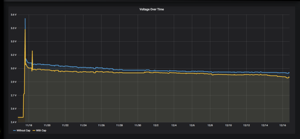
You might notice, that there is no significant difference in the development of both units. If anything, the unit with the cap might drain the battery just slightly faster than the other. Now imagine if the devices were attached to a window, which typically gets opened no more than 2 - 4 times a day, as opposed to a door of a frequently used room, the discrepancy might be more noticeable since the duty cycle is much lower / time between wake ups much higher, possibly resulting in the (electrolytic) cap being the largest load of the device.
But I have to admit that I have no long-time data. It is possible, that the capacitor might make a huge difference once the battery voltage drops below 2.3V or something like that.But is the device with the capacitor more reliable (so far)? Well, have a look at another boring graph:

This graphs displays a dot whenever a device woke up and transmitted a state change over the course of two days. (I made the blue dots a little bigger because they have a lower z-index / are visually behind the yellow ones). Looks like there is no event that has been reported by only one device.
I know, it’s just my personal experience and observation and doesn’t mean much. I guess, it wouldn’t hurt to use a 100 µF MLCC instead of a 10 - 22 µF one, considering that their leakage current is way, way below that of a good electrolytic cap. But regarding the current MLCC shortage - getting your hand on a decent 100 µF MLCC isn’t easy nor cheap. A quick look at Mouser reveals twelve MLCCs with a voltage rating of 6.3 VDC and only one with 10 VDC or above at stock (only looking at 0805 and 1206/1210 packages). Most of them only in 3-digit quantities with prices over 1 EUR / 1.15 USD or more per 100. Not the best time to go that route. Adding up a bunch of smaller capacity ones might be a decent workaround (but requires getting another revision of the board manufactured first, while the first hasn't even arrived yet :D ).
Antenna and ICSP positioning
I tried to keep any copper away from the antenna - maybe I can do a better job, that’s true. I also don’t plan to solder headers onto it if you are worried the pins might interfere with the signal.
Low power LED
Could you please suggest / link a LED such as you are using? Just to give me an idea what to look for regarding their specs.
Placing the battery on the bottom layer
I’ve thought about that, too. And it would make sense considering the large ground plane on the bottom that I am currently connecting to the battery through three little vias. But there’s only ~17mm of depth on the windows in my house where I’d like to fit in the device as well as the magnet. The thickness is probably the most critical dimension of all. I’ll take this into consideration - another point on my to-do list. :)
-
Thank you very much for your answer, @Nca78!
Sorry for another lengthy post. I try to keep it short but still being relevant and informative. Feel free to skip to the section(s) that interest you.
Regarding the additional capacitor to deal with the current spikes
When I started this thread, I also cobbled together two prototypes that I attached to the same door.
- 3V CR2032 coin cell (Sony)
- Atmega328P-PU with two 0.1 µF ceramics and 10kΩ pull-up on reset
- NRF24L01+ with one 0.1 µF ceramic
- 3mm led with 1kΩ resistor as an indicator
- mechanical reed switch with a 1M Ω pull-up resistor
They are both identical, except for one additional 220 µF electrolytic cap (it’s a nichicon ULD series cap) on one device in parallel to the battery to compare how this affects reliability and the battery consumption. (I also asked a question on the ElectricalEngineering StackExchange on that topic if you are interested: Protecting a coin cell from high current spikes - using a capacitor or not?)
Have a look at this graph that displays the measured voltage over time. (Ignore the spikes at the beginning - that was me being stupid).

You might notice, that there is no significant difference in the development of both units. If anything, the unit with the cap might drain the battery just slightly faster than the other. Now imagine if the devices were attached to a window, which typically gets opened no more than 2 - 4 times a day, as opposed to a door of a frequently used room, the discrepancy might be more noticeable since the duty cycle is much lower / time between wake ups much higher, possibly resulting in the (electrolytic) cap being the largest load of the device.
But I have to admit that I have no long-time data. It is possible, that the capacitor might make a huge difference once the battery voltage drops below 2.3V or something like that.But is the device with the capacitor more reliable (so far)? Well, have a look at another boring graph:

This graphs displays a dot whenever a device woke up and transmitted a state change over the course of two days. (I made the blue dots a little bigger because they have a lower z-index / are visually behind the yellow ones). Looks like there is no event that has been reported by only one device.
I know, it’s just my personal experience and observation and doesn’t mean much. I guess, it wouldn’t hurt to use a 100 µF MLCC instead of a 10 - 22 µF one, considering that their leakage current is way, way below that of a good electrolytic cap. But regarding the current MLCC shortage - getting your hand on a decent 100 µF MLCC isn’t easy nor cheap. A quick look at Mouser reveals twelve MLCCs with a voltage rating of 6.3 VDC and only one with 10 VDC or above at stock (only looking at 0805 and 1206/1210 packages). Most of them only in 3-digit quantities with prices over 1 EUR / 1.15 USD or more per 100. Not the best time to go that route. Adding up a bunch of smaller capacity ones might be a decent workaround (but requires getting another revision of the board manufactured first, while the first hasn't even arrived yet :D ).
Antenna and ICSP positioning
I tried to keep any copper away from the antenna - maybe I can do a better job, that’s true. I also don’t plan to solder headers onto it if you are worried the pins might interfere with the signal.
Low power LED
Could you please suggest / link a LED such as you are using? Just to give me an idea what to look for regarding their specs.
Placing the battery on the bottom layer
I’ve thought about that, too. And it would make sense considering the large ground plane on the bottom that I am currently connecting to the battery through three little vias. But there’s only ~17mm of depth on the windows in my house where I’d like to fit in the device as well as the magnet. The thickness is probably the most critical dimension of all. I’ll take this into consideration - another point on my to-do list. :)
@bearwithbeard said in Novice requesting PCB review and advice for a window / door sensor:
I know, it’s just my personal experience and observation and doesn’t mean much. I guess, it wouldn’t hurt to use a 100 µF MLCC instead of a 10 - 22 µF one, considering that their leakage current is way, way below that of a good electrolytic cap. But regarding the current MLCC shortage - getting your hand on a decent 100 µF MLCC isn’t easy nor cheap. A quick look at Mouser reveals twelve MLCCs with a voltage rating of 6.3 VDC and only one with 10 VDC or above at stock (only looking at 0805 and 1206/1210 packages). Most of them only in 3-digit quantities with prices over 1 EUR / 1.15 USD or more per 100. Not the best time to go that route. Adding up a bunch of smaller capacity ones might be a decent workaround (but requires getting another revision of the board manufactured first, while the first hasn't even arrived yet ).
You can have a look here for some explanation about calculation of capacitor value
http://www.ti.com/lit/wp/swra349/swra349.pdfI didn't buy capacitors recently, didn't notice the availability/price problem, this is creepy, I'm happy to have stocks.
I just check on an order made last year on Arrow, only 2 cap references are still available for sale, one is 80% more expensive, the other over 300% more :cry: -
Thanks again, @Nca78. I must have skipped the capacitor dimensioning part when I read that white paper a while ago. :thinking_face:
Fiddling around with some numbers both at the lower and higher end of their expected scale, yes, 100µF seems to be a save capacity to go for.
And let's be honest - since I'm planing to use a MLCC instead of the electrolytic cap there is no (technical) reason to leave it out or undersize it.
Thank you @momo90!
Yes, I intend to do so once I got them up and running. -
well,,i buy some hall effect sensor as EM-1781-T5,HAL2481L,ES248L, work well,but battery cost too much for me ,the EM-1781-T5 consume least,atmega328p 1MHZ with sleep nothing sensors 7.8ua,work with EM1781 sleep 16ua,when Magnetic near,cost 22ua, .......so ....i think Although it provides a more accurate and wider range of sensing, it consumes much more than a reed.
-
Hi @huex,
you might want to give the DRV5032FB from TI a chance, which I've listed in my opening post. The data sheet states an average power consumption of 0.69µA at 3V.
I only found a Japanese data sheet for the EM-1781 (which you mentioned as the sensor which has the least current consumption), but as far as I understand, it specifies an average consumption of 6.5µA at 1.85V. At 3V it is properly even more. That's ten times higher than the DRV5032FB.
The DRV5032FB should consume less than a reed switch, since it doesn't require pull-ups to keep the interrupt pin from floating. Even with a rather high 1MΩ resistor you'd look at ~3µA at 3V using a reed switch.
Also - Let's not forget that reed switches tend to bounce which needs to be counteracted in software or it triggers multiple times. Both cases increase power consumption since the device spends more time in an active state. They are also a mechanical part - the more often you use them, the higher is the chance that they fail.
I still think, overall, a hall effect switch is the better option for this application
@bearwithbeard
YEAH,because difficulty get dr5032FB in my region,more 20HZ with 3v like DRV5032AJD,DRV5032ZEDBZR ,DRV5032FA Available ,maybe other similar low power and low voltage chips ? -
No, unfortunately there are no equally suitable alternatives I know off. There's actually only one that meets these requirements:
- Supply voltage at least between 2V and 3.3V
- Average current consumption < 2µA
- Push-pull output
- Preferably omnipolar
The closest alternatives I know of are the Honeywell SL353LT and the Diodes AH1911. The former can only operate down to 2.2V unfortunately and the latter, while meeting all requirements, drains 1.6µA in average, which is twice as much as the TI chip consumes - but it might be a good alternative for you if it is more easily available in your region.
-
No, unfortunately there are no equally suitable alternatives I know off. There's actually only one that meets these requirements:
- Supply voltage at least between 2V and 3.3V
- Average current consumption < 2µA
- Push-pull output
- Preferably omnipolar
The closest alternatives I know of are the Honeywell SL353LT and the Diodes AH1911. The former can only operate down to 2.2V unfortunately and the latter, while meeting all requirements, drains 1.6µA in average, which is twice as much as the TI chip consumes - but it might be a good alternative for you if it is more easily available in your region.
@bearwithbeard why would you need to go below 2.2V if you're powering your board with a CR2032 ? At 2.5V it will nearly be dead already, with only a few % of capacity left.
And a NO/NC reed switch can be used to have very low power consumption, and at every change of status you switch the pin you are watching with the interrupt. It's a 0uA standby power consumption, but I still prefer the DRV5032 because of the small size and robustness, reed switches are bulky and fragile, especially the NO/NC with their dual pins on one side.
I have looked a lot and didn't find anything better than DRV5032, second best choice is indeed SL353LT. If you don't have any source for your region you can still order at lcsc, they have a few (7). Unfortunately their DRV5032 are not FB versions, but they have a push-pull version in stock so you will get the same power consumption as SL353LT. If I'm not wrong all versions can go as low as 1.65V so it's suitable for you. There's nothing lower than 1.5uA except the drv5032FB.
-
@bearwithbeard why would you need to go below 2.2V if you're powering your board with a CR2032 ? At 2.5V it will nearly be dead already, with only a few % of capacity left.
And a NO/NC reed switch can be used to have very low power consumption, and at every change of status you switch the pin you are watching with the interrupt. It's a 0uA standby power consumption, but I still prefer the DRV5032 because of the small size and robustness, reed switches are bulky and fragile, especially the NO/NC with their dual pins on one side.
I have looked a lot and didn't find anything better than DRV5032, second best choice is indeed SL353LT. If you don't have any source for your region you can still order at lcsc, they have a few (7). Unfortunately their DRV5032 are not FB versions, but they have a push-pull version in stock so you will get the same power consumption as SL353LT. If I'm not wrong all versions can go as low as 1.65V so it's suitable for you. There's nothing lower than 1.5uA except the drv5032FB.
@nca78
As I stated in the opening post, I’ve just started getting into electronics and programming a few month ago - I don’t know a lot, but I try to try to get the best out of if. (And that’s also the reason why i’m always thankful for advice, critique and suggestions.)In general, I thought it would be a good idea to use components that are capable to work in a wider voltage range than the power source can provide, instead of the other way around.
I am aware that most of the usable capacity of a CR2032 is exhausted long before it drops down to 2V. But at the same time, almost all fabricators state that they consider the battery to be “dead” at 2V. So, with the little experience I have, I ask myself, why would I want to waste the ~5% capacity that is left between 2.5V and 2V from the beginning? This might be a few weeks or even just a few days of extended lifetime, but it comes at no extra cost.
Maybe I should consider looking for alternatives to a CR2032 that don’t increase the overall size and complexity of the circuit too much. Using a CR2450 (~600mAh) would increase the overall thickness by merely 2mm, but increase the expected life time by a factor of ~2.5. Boosting a single LR03 to 2.5V or 3V might not be worthwhile despite its relatively large capacity.
And a NO/NC reed switch can be used to have very low power consumption, and at every change of status you switch the pin you are watching with the interrupt.
I have only worked with regular NO reed switches - didn’t know there are SPDT-type reed switches available. Nice! Then again, if you buy this kind of reed switches from reputable distributors instead of noname grab bags from China, they cost (a lot) more than a DRV5032FB (Mouser lists them between 2.7 and 10+ USD a piece) and you still have to deal with all the disadvantages of a reed switch that have already been mentioned.
Oh, btw - I just stumbled upon the Honeywell SM351LT / SM353LT. Works between 1.65 - 5.5V and is advertised with an average current consumption of ~350nA.
I guess, that can only be achieved when supplied with a very low input voltage since the data sheet states a sleep current of 0.2µA at 1.8V and 2.6µA at 5.5V. Too bad it doesn’t provide numbers for 3V.On top of that, with a sensitivity of 7 resp. 14 Gs it would be possible to use very small magnets. Even a tiny 3x2mm N38 grade neodymium disc magnet would be strong enough to trigger at a distance of 10mm.
-
@nca78
As I stated in the opening post, I’ve just started getting into electronics and programming a few month ago - I don’t know a lot, but I try to try to get the best out of if. (And that’s also the reason why i’m always thankful for advice, critique and suggestions.)In general, I thought it would be a good idea to use components that are capable to work in a wider voltage range than the power source can provide, instead of the other way around.
I am aware that most of the usable capacity of a CR2032 is exhausted long before it drops down to 2V. But at the same time, almost all fabricators state that they consider the battery to be “dead” at 2V. So, with the little experience I have, I ask myself, why would I want to waste the ~5% capacity that is left between 2.5V and 2V from the beginning? This might be a few weeks or even just a few days of extended lifetime, but it comes at no extra cost.
Maybe I should consider looking for alternatives to a CR2032 that don’t increase the overall size and complexity of the circuit too much. Using a CR2450 (~600mAh) would increase the overall thickness by merely 2mm, but increase the expected life time by a factor of ~2.5. Boosting a single LR03 to 2.5V or 3V might not be worthwhile despite its relatively large capacity.
And a NO/NC reed switch can be used to have very low power consumption, and at every change of status you switch the pin you are watching with the interrupt.
I have only worked with regular NO reed switches - didn’t know there are SPDT-type reed switches available. Nice! Then again, if you buy this kind of reed switches from reputable distributors instead of noname grab bags from China, they cost (a lot) more than a DRV5032FB (Mouser lists them between 2.7 and 10+ USD a piece) and you still have to deal with all the disadvantages of a reed switch that have already been mentioned.
Oh, btw - I just stumbled upon the Honeywell SM351LT / SM353LT. Works between 1.65 - 5.5V and is advertised with an average current consumption of ~350nA.
I guess, that can only be achieved when supplied with a very low input voltage since the data sheet states a sleep current of 0.2µA at 1.8V and 2.6µA at 5.5V. Too bad it doesn’t provide numbers for 3V.On top of that, with a sensitivity of 7 resp. 14 Gs it would be possible to use very small magnets. Even a tiny 3x2mm N38 grade neodymium disc magnet would be strong enough to trigger at a distance of 10mm.
@bearwithbeard yes I notice you make a lot of efforts to study all the options, I'm impressed of the care you put on your board !
And yes it's always a good idea to take some margin but how much lifetime will those 5% get you ? Somewhere like 1 month for a 2 years battery life, it's not really a game changer. What I meant is it's probably better to chose a sensor with a tiny lower power consumption and 2.2V instead of 1.8V as it will save more energy than you can gain with those last 5%.
I agree with you for the other battery options, CR2450 is a big increase in battery life and if you accept to have one dimension of at least 30-32mm (battery + radio antenna clear from it) then it's worth it. There are ultra low power boosters like TPS6109x that provide better battery life from a single LR03, but it is relatively expensive (few extra $) and takes around 1sq cm of board space (IC, inductance, 3 caps, 2 resistors). So it fails on most of the points: higher complexity, higher cost, and much more bulky with AAA.
Thank you for the tip for SM351/353, I didn't knew about it. Sensibility is really impressive, I have already added some to my list for my next purchase, I will test and report the consumption at 3V. Hope it's closer to the one at 1.8V than 5.5V, but I'm not optimistic when I see the quick increase from 1.65V to 1.8V (9% more voltage = 25% more current).
And for the reed switches, yes not worth all the pain to save at best 0.2-0.3$ if you buy them from AliExpress.
-
Sorry for taking so long to reply. I’m spending some quality time with my family these days and try to relax a bit. I hope you all can share some time with your loved ones as well.
@nca78 I agree with you that it would be better to choose a sensor with a lower power consumption, if it can only work down to 2.2V. I implicitly assumed that there is no sensor that’s more economical than the DRV5032FB, which happens to work down to 1.65V or something, so I chose it as my benchmark. Sorry for not making myself clear earlier!
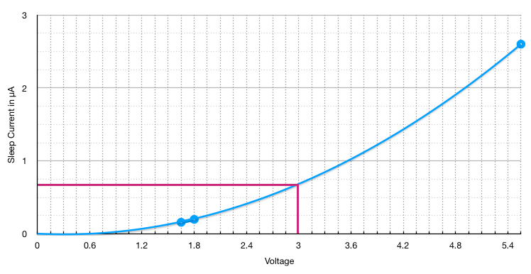
Regarding the Honeywell sensor: I quickly put the sleep current values from the datasheet in a spreadsheet and plotted a graph trough those points. Assuming the current increases uniformly, we should expect 0.67µA at 3V, in which case it would match the DRV5032FB in terms of power consumption. Let's hope it's not far off from that, because the higher sensitivity would make it the better choice if that's needed.
And again, thanks for your participation. Really appreciated.
In the meantime I’m slowly making progress on a “rev 2” board that also implements some suggestions that came from you guys. I aim to post an update before the new year begins.
-
It took me a little bit longer to post an update, but I decided to spend some more time with my family and focused on another project for a while. Hope you've all had a good start into the new year!
I made quite a lot of changes to the PCB and incorporated ideas and suggestions from you guys.
As always - feel free to skip whatever section you don't care about or just read the headings to get a "tl;dr" version of the changes. :stuck_out_tongue_winking_eye:
Schematic and PCB layout
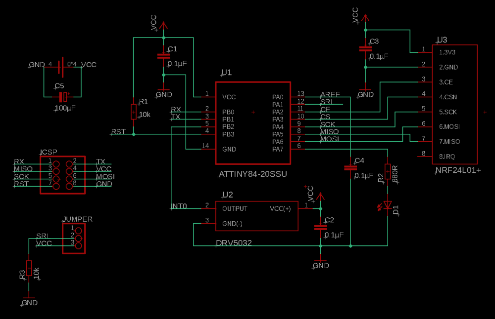
Schematic
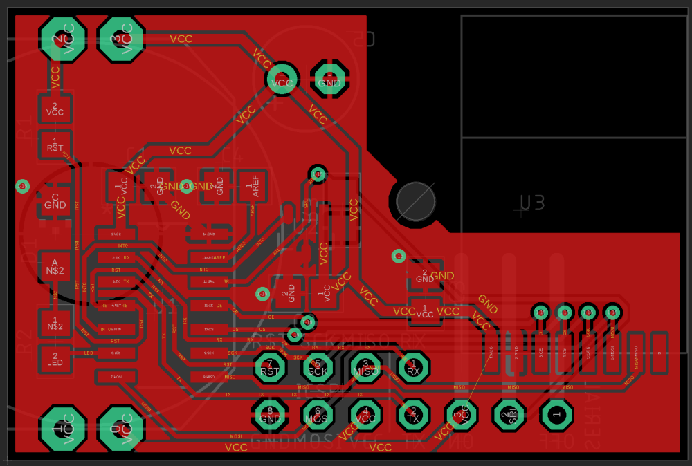
Top Layer
Bottom Layer
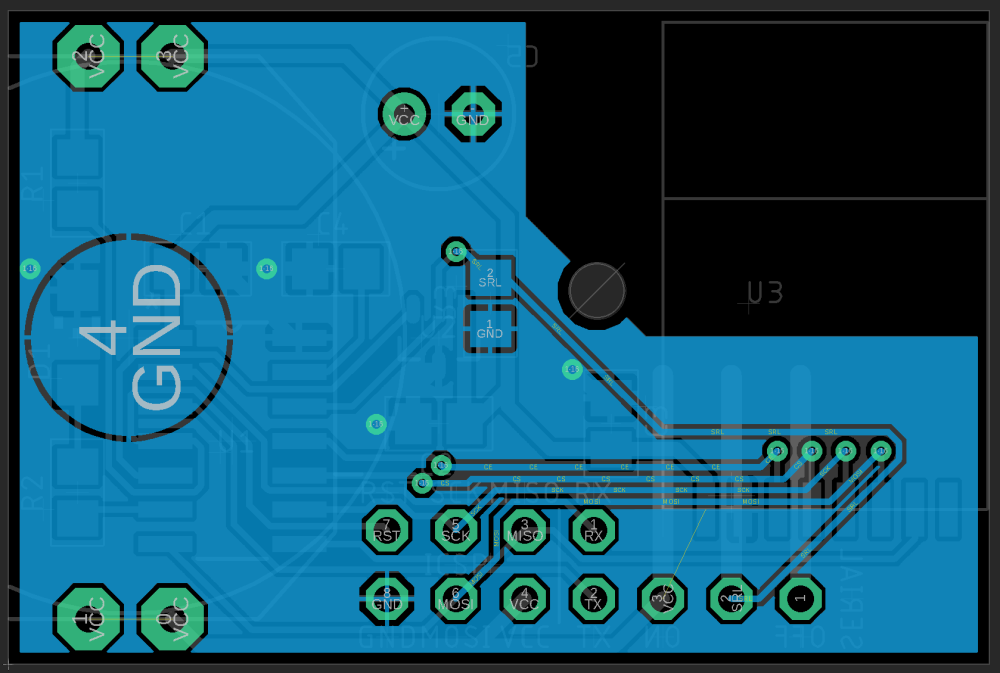
The routing around the Attiny's pins almost looks like I'm working with a single-layer PCB, but I can't use vias except for GND in this area as the coin cell occupies the whole backside (and several (inexpensive) PCB manufactures seem to be unable to make tented vias and cover them with a solder resist mask). I guess those fancy "spirals" around the left-hand pins won't cause any issues.
Trace width for GND and VCC is still 20 mil. All other signals are now 9 instead of 10mil.
There are some airwires visible between some of the VCC signals. I guess EAGLE doesn't understand that the four VCC through-hole pads of the battery holder are physically connected. If anyone could tell me how to deal with it, that would be greatly appreciated!
(And yes, yes. That lonely resistor on the back looks so sad and silly. But it's the position with the shortest routes and least vias I could come up with, so it seems to be the best solution.)
List of Components
- U1: Attiny84A-SSU
- U2: TI DRV5032FB or Honeywell SM353LT
- U3: NRF24L01+ SMD module
- R1, R3: 10kΩ (0805)
- R2: 680Ω (0805)
- D1: Kingbright 2 mA, 150mcd, 40 deg, red Dome-LED (1206)
- C1, C2, C3, C4: 0.1µF 50VDC X7R MLCC (0805)
- C5: 100µF 16VDC electrolytic cap (e.g. Nichicon UMA series)
I will focus on the Attiny variant for now
I prefer using the Attiny84 for several reasons over the Atmega328P for this project - it allows to make the overall device a little bit smaller, gives more options for routing signals and costs less than half of an 328P, which feels wasteful to use with most of its pins unconnected.
I will most likely go back into EAGLE and design a variant for the Atmega328P as well before I'm going to order PCBs the next time so that I get a batch of both anyway - but I don't want to continue working on two variants simultaneously while major changes are likely.
Ground plane on both PCB layers
As suggested by @Nca78, I've also added a ground plane on the top layer this time.
But I'm unsure if this has any consequences for the decoupling capacitors and their corresponding power pins. Doesn't it "break" their current loop? Why would it be considered bad if the plane would be VCC instead? (I definitely need some good reading on this topic.)
Status LED included
@Nca78 pointed out that there are SMD LEDs that can produce a bright spotlight with very little power.
Mouser doesn't seem to have any LED in their catalogue with a current consumption <2mA that's larger than 0402. So the one I chose to include is a 1206 dome-LED from Kingbright which reaches a luminosity of 150mcd at 2mA in a 40° cone. LEDs with similar specs seem to be easily available. I think that should do the job.
Added serial pins and a jumper
Originally, I didn't want to add a serial header at all, as it would take up way to much space on the PCB. But @mfalkvidd made me think about a simpler solution: Adding RX/TX pins to the already existing ICSP header.
This allows for on-demand debugging functionality via software serial if pin 12 is pulled high through the jumper. If the jumper is disconnected, pin 12 will get pulled down to ground and serial functionally will be disabled, going back to normal operation mode and reducing power consumption to a minimum.
At this point, I don't worry about auto-reset functionality, since the Attiny84 with its 8kB of flash memory hasn't enough space to fit a bootloader besides the actual program.
That's a consideration to take into account with the Atmega variant.Increased distance between antenna and copper
The new design leaves much more space between the antenna of the NRF24 module and any part of the circuit (at least 5mm). The closest metal part will be a M2 bolt that attaches the board to the enclosure.
Using an electrolytic capacitor as a buffer instead of a MLCC
Well ... I went forwards and backwards many times whether to use an electrolytic cap or an MLCC. After all, I concluded using an electrolytic cap is the most sensible solution. Here's my (lengthy) explanation for it:
-
(Large capacity) MLCCs are increasingly difficult to acquire and their prices are going up as well. There is no guarantee that I - or anyone else interested in this project, as private individuals - can get an affordable MLCC in a specific SMD package in a reasonable amount of time. Items that are in stock today can be sold out by tomorrow, with lead times of "53 weeks".
-
The actual capacitance of MLCCs is largely dependent on the applied voltage in relation to its rated voltage (DC bias, some background info). This means that a 100µF MLCC rated for 10VDC might store a charge of only 40 - 70µF when supplied with 3V (average values I've gotten by looking through the online databases from murata and TDK). This would require the use of a MLCC that has a higher nominal capacitance or possibly, depending on the specific part, a higher rated voltage, which has its "sweet spot" at around 3V. But those cost easily 5 - 25 USD / Euro a piece. That's not sensible at all.
-
Last but not least: Reading a paper from a German battery manufacturer ("Leakage current properties of modern electrolytic capacitors"), I concluded that using an electrolytic cap in battery-powered applications might not be as bad as one might think.
AVX apparently released a paper very similar to this, but unfortunately it doesn’t seem to be (publicly) available anymore. Rubycon writes in a technical note that the specified leakage currents are higher than they actually are, “because it takes too much time to measure the true leakage current”.
Summarizing, the specified leakage current in a capacitors data sheet is usually far above the actual operating leakage current that should be expected when a voltage is applied to the capacitor continuously. It is generally by a few factors lower than specified, even more so when the supply voltage is far below the rated voltage (TDK, p. 17) - for a 100µF 16VDC cap and a specified leakage current of up to 3µA that is supplied with 3V, the operating leakage current should settle between 100 and 250nA.
Plus, my experiment with the two prototypes I mentioned in an earlier post seems to back the point that the leakage current of (decent) electrolytic caps isn't a huge deal in low power applications as one might think, since both devices seem to drain the battery equally.
Considering that 100µF 16VDC electrolytic caps with a total height below 5.5mm are - other than similar MLCCs - rather cheap and widely available, it seems reasonable to stick with an electrolytic cap as a buffer.
After all, the limiting factor regarding the total uptime of this device isn't the technology of the buffer capacitor - it's the self-imposed constraint in regards to the overall dimensions of the device, thus opting for a tiny CR2032 coin cell. Choosing a slightly larger power source will absolutely have a much bigger impact on the battery life as any kind of capacitor could have.
Yes, the best possible capacitor might increase the battery life by a few weeks or even two months - a CR2450 instead of a CR2032 would increase it by years.
For the sake of completeness, there are also specific "low leakage" electrolytic caps available like the UKL series from nichicon which specify a leakage current of less than 0.2µA after two minutes. Unfortunately, with a minimal size of 6.3mm x 11mm they are a bit too large for this project.
Moved the battery to the back of the PCB
Making use of the fact that I go back to using a electrolytic cap as a buffer, I can mount the battery as well as the cap to the back of the PCB - as well as the 90° angle pin header for the jumper that otherwise wouldn't fit on the board.
This makes the device ~2mm thicker (~9mm total thickness) than mounting everything on the top of the PCB (~7mm total thickness) but I can keep the board dimensions of 24mm x 36mm despite adding more components. Having all the thick components on the back also means that the hall effect sensor is as close to the front of the enclosure as possible, reducing the distance to the magnet.
The CR2032 can easily be replaced by a CR2450, which has a three times higher nominal capacity, without increasing the overall device thickness and only increasing the PCB height from 24mm to 27mm - I just have to commit to using a specific coin cell holder model to adjust the contacts on the PCB accordingly. Until then, I'll stick with the CR2032.
That's it for now. Your comments, ideas and suggestions are highly appreciated, as always. Thanks for your attention!

